

Semiconductor sealing silicone composition and semiconductor device
a silicone composition and semiconductor technology, applied in the direction of semiconductor/solid-state device details, transportation and packaging, synthetic resin layered products, etc., can solve the problems of large workability constraints, partial scorching on the surface, and scalding, etc., to achieve rapid cure, adequate working time, and suitable for screen printing applications
- Summary
- Abstract
- Description
- Claims
- Application Information
AI Technical Summary
Benefits of technology
Problems solved by technology
Method used
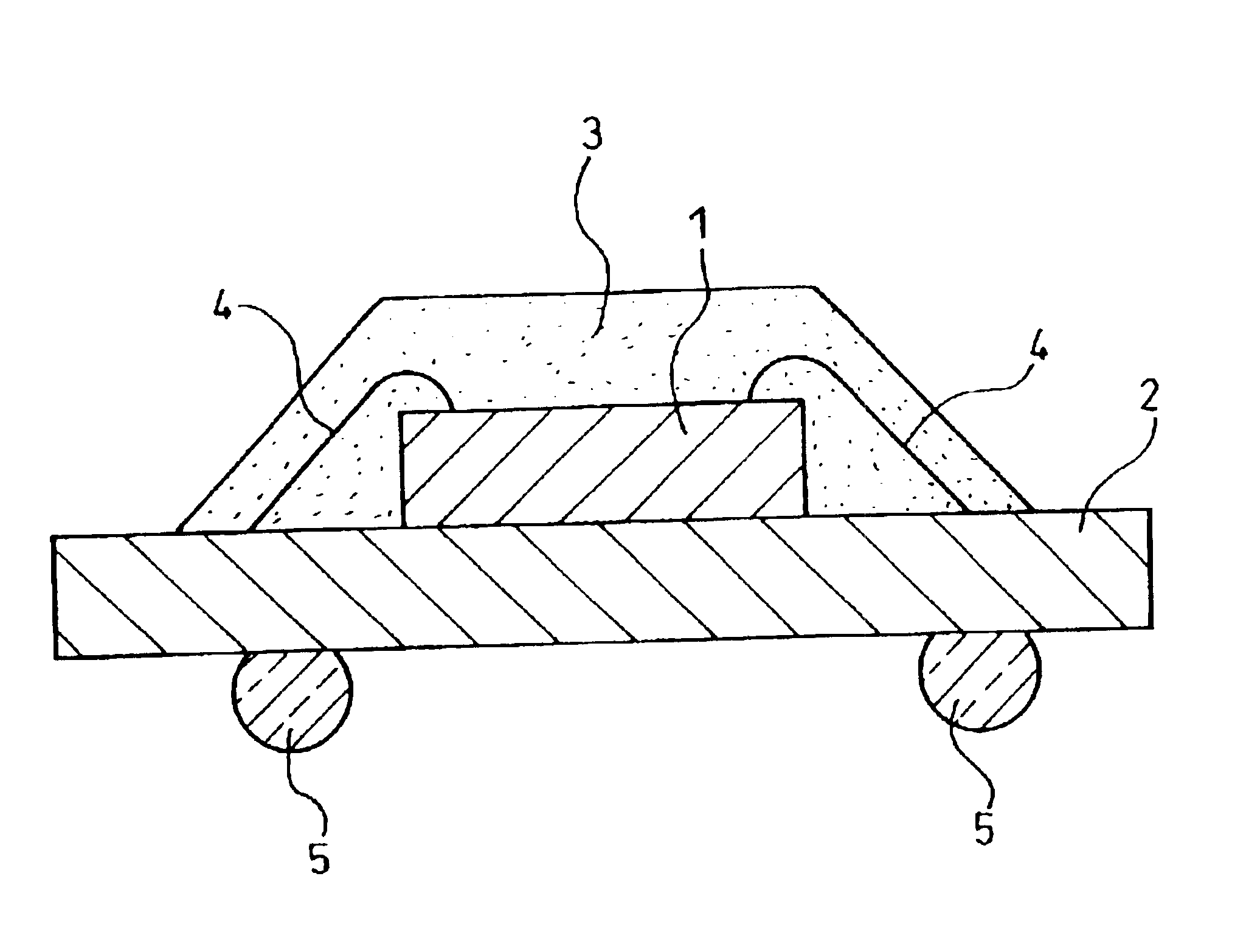
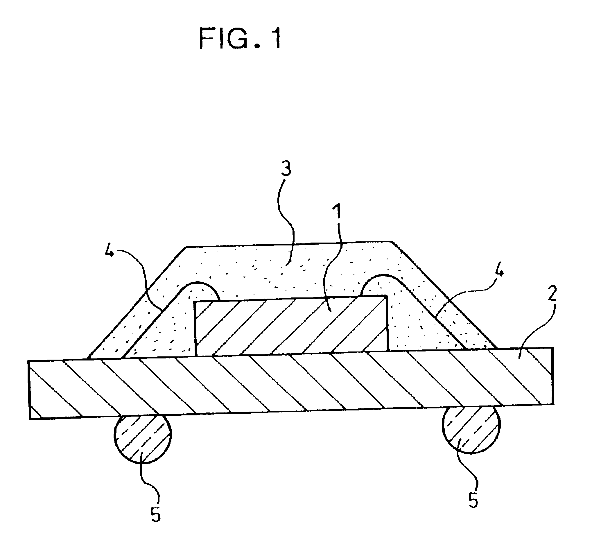
Image

Examples
example 1
[0053]A mixture of (A) 100 parts by weight of a dimethylpolysiloxane with both terminals of the molecular chain blocked with dimethylvinylsiloxy groups (with a vinyl group content within the dimethylpolysiloxane of 0.0053 mol / 100 g) and with a viscosity of 5,000 mPa·s, (B) 3.6 parts by weight of a methylhydrogenpolysiloxane with both terminals of the molecular chain blocked with trimethylsiloxy groups (with a quantity of hydrogen atoms bonded to silicon atoms (SiH groups) within the methylhydrogenpolysiloxane of 0.3 mol / 100 g) (producing a molar ratio H / Vi (hereafter this abbreviation is used) of the number of SiH groups within the constituent (B) relative to the number of vinyl groups within the constituent (A) of 2.0 mol / mol), (C) 0.3 parts by weight of an isocyanurate modified silicone additive represented by a formula shown below,
(D) 0.1 parts by weight of a 2-ethylhexylalcohol solution of chloroplatinic acid (2% by weight) (producing an equivalent of 20 ppm of platinum metal r...
example 2
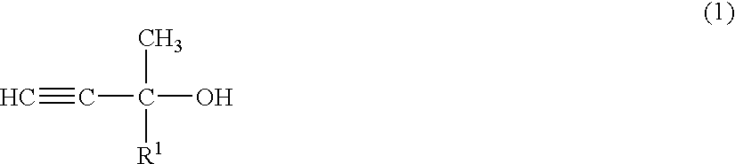
[0057]With the exceptions of using 1.0 parts by weight of an epoxy group containing hydrogensiloxane represented by a formula shown below as the constituent (C),
and 0.4 parts by weight (a molar ratio of 347 relative to the quantity of platinum metal of the constituent (D) described in the example 1) of a compound represented by a formula shown below as the constituent (E),
an addition curing type silicone sealant was prepared and then evaluated in a similar manner to the example 1.
example 3
[0058]With the exceptions of reducing the quantity of the constituent (B) to 1.0 parts by weight (H / Vi=0.6 mol / mol), using 3.0 parts by weight of a partial hydrolysate of trimethoxysilane, represented by an average formula shown below, as the constituent (C),
and increasing the quantity of the constituent (E) to 0.4 parts by weight (a molar ratio of 397 relative to the quantity of platinum metal of the constituent (D) described in the example 1), an addition curing type silicone sealant was prepared and then evaluated in a similar manner to the example 1.
PUM
| Property | Measurement | Unit |
|---|---|---|
| molar ratio | aaaaa | aaaaa |
| boiling point | aaaaa | aaaaa |
| molar ratio | aaaaa | aaaaa |
Abstract
Description
Claims
Application Information