Flip-chip light emitting diode with resonant optical microcavity

a light-emitting diode and flip-chip technology, applied in the direction of basic electric elements, semiconductor devices, electrical apparatus, etc., can solve the problems of large number of layers, increased electrical resistance losses, and limited nitride led performance extraction of light from semiconductors, etc., to achieve enhanced efficiency, easy extraction from the device, and enhanced light emission

Inactive Publication Date: 2005-11-29
NAT TECH & ENG SOLUTIONS OF SANDIA LLC
View PDF13 Cites 106 Cited by
  • Summary
  • Abstract
  • Description
  • Claims
  • Application Information

AI Technical Summary

Benefits of technology

[0012]The present invention relates to a flip-chip light emitting diode with enhanced efficiency. The device structure employs a microcavity structure in a flip-chip configuration. The microcavity enhances the light emission in vertical modes, which are readily extracted from the device. Most of the rest of the light is emitted into waveguided lateral modes. Flip-chip configuration is advantageous for light emitting diodes (LEDs) grown on dielectric substrates (e.g., gallium nitride LEDs grown on, sapphire substrates) in general due to better thermal dissipation and lower series resistance. Flip-chip configuration is advantageous for microcavity LEDs in particular because (a) one of the reflectors is a high-reflectivity metal ohmic contact that is already part of the flip-chip configuration, and (b) current conduction is only required through a single distributed Bragg reflector. Some of the waveguided lateral modes can also be extracted with angled sidewalls used for the interdigitated contacts in the flip-chip configuration.

Problems solved by technology

One of the primary limitations to nitride LED performance is extracting light from the semiconductor.
The problem is that semiconductors generally have large refractive indices (n).
A larger number of layers could increase electrical resistance losses due to the large number of interfaces or if some of the layers are difficult to dope.
Also, it might be difficult to maintain material quality with a larger number of layers—particularly if the layers do not have the same lattice constant.
Distributed Bragg reflectors are particularly difficult to fabricate for alloys of aluminum-indium-gallium-nitride (AlInGaN), because the Al-alloys are difficult to dope (p-type is more difficult than n-type), and because there is a large lattice mismatch between AlGaN and GaN compounds.
Secondly, the flip-chip geometry has lower series resistance compared to a front-emission geometry because a thicker metal p-contact pad can be used as a current spreader (front-surface emission requires an optically-transparent p-contact pad to transmit the light, which requires a very thin metal layer).

Method used


Image

  • Flip-chip light emitting diode with resonant optical microcavity
  • Flip-chip light emitting diode with resonant optical microcavity
  • Flip-chip light emitting diode with resonant optical microcavity

Examples


Embodiment Construction

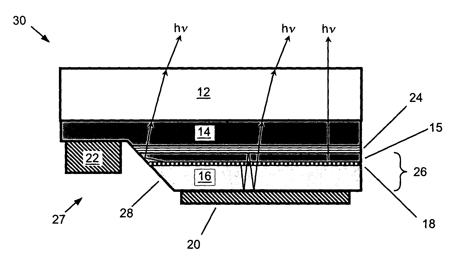
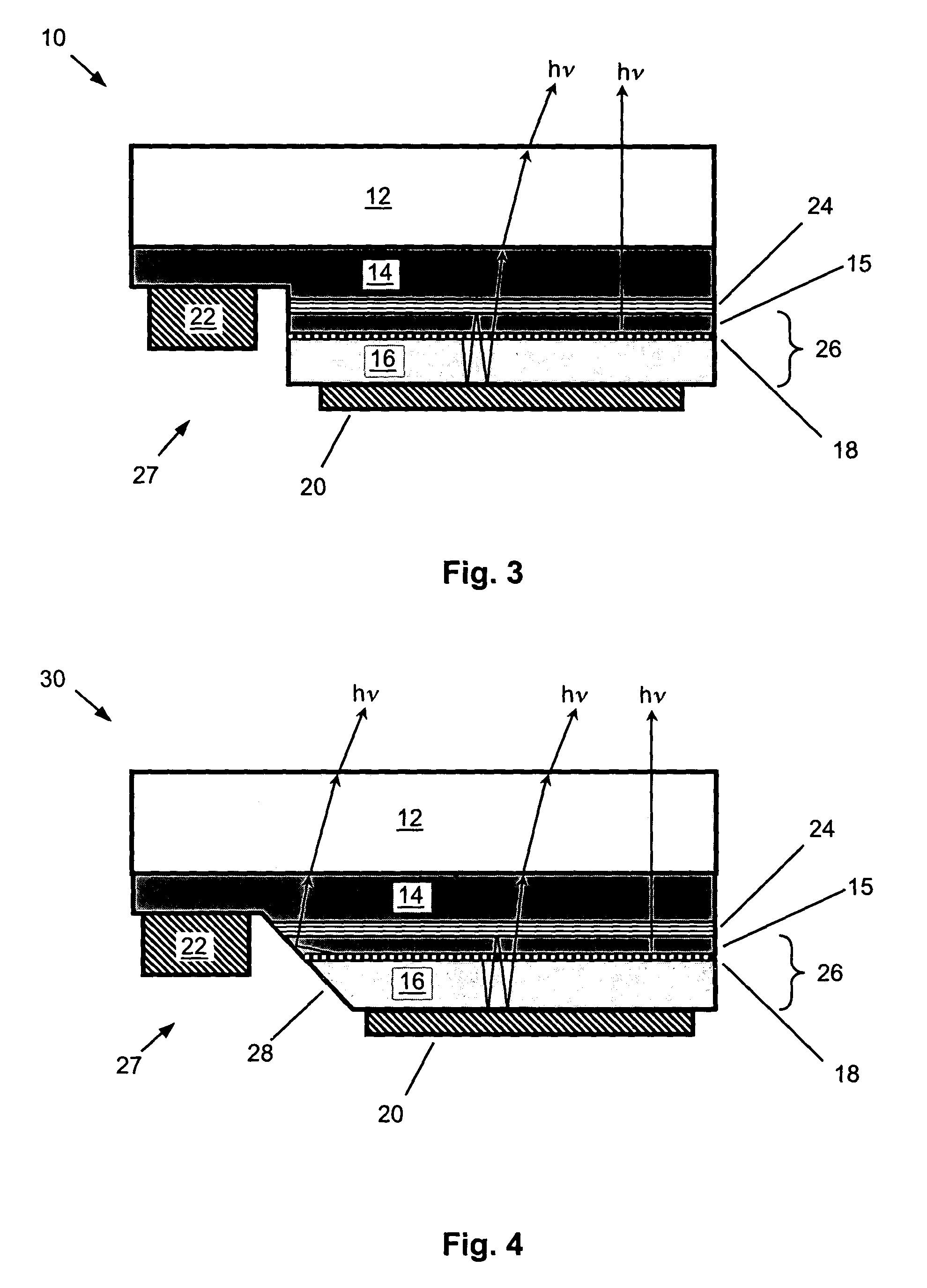
[0018]Note that in the drawings, the thicknesses of the various layers of insulating, semiconductor, and metallic materials; and other dimensions, such as the width of contact pads, are not drawn to scale, but, rather, are shown schematically for purposes of illustration and easy identification.

[0019]FIG. 3 shows a schematic cross-section view of a first example of a flip-chip LED with a resonant microcavity, according to the present invention. Flip-chip LED 10 comprises a transparent growth substrate 12 (e.g., sapphire). First n-doped buffer layer 14 (e.g., n-GaN) overlays substrate 12. Partially reflective mirror layer 24 overlays the first n-type buffer layer 14. Second n-doped barrier layer 15 (e.g., n-GaN) overlays partially reflective mirror layer 24. Light emitting active layer 18 overlays second n-doped barrier layer. P-doped barrier layer 16 (e.g., p-GaN) overlays light emitting active layer 18. Light emitting active layer 18 resides in-between second n-doped barrier layer ...


PUM


Abstract

A flip-chip light emitting diode with enhanced efficiency. The device structure employs a microcavity structure in a flip-chip configuration. The microcavity enhances the light emission in vertical modes, which are readily extracted from the device. Most of the rest of the light is emitted into waveguided lateral modes. Flip-chip configuration is advantageous for light emitting diodes (LEDs) grown on dielectric substrates (e.g., gallium nitride LEDs grown on sapphire substrates) in general due to better thermal dissipation and lower series resistance. Flip-chip configuration is advantageous for microcavity LEDs in particular because (a) one of the reflectors is a high-reflectivity metal ohmic contact that is already part of the flip-chip configuration, and (b) current conduction is only required through a single distributed Bragg reflector. Some of the waveguided lateral modes can also be extracted with angled sidewalls used for the interdigitated contacts in the flip-chip configuration.

Description

FEDERALLY SPONSORED RESEARCH[0001]The United States Government has rights in this invention pursuant to Department of Energy Contract No. DE-AC04-94AL85000 with Sandia Corporation.BACKGROUND OF THE INVENTION[0002]The present invention relates generally to a light emitting diode (LED), and more specifically to a flip-chip light emitting diode with resonant microcavity for enhanced light extraction efficiency.[0003]A light emitting diode (LED) is a semiconductor device that generates light from electrical excitation. It would be advantageous for many applications to improve the efficiency (radiant power out divided by electrical power in) of LEDs. One of the primary limitations to nitride LED performance is extracting light from the semiconductor. The problem is that semiconductors generally have large refractive indices (n). The large refractive index causes most of the light to be internally reflected at the front surface due to total internal reflection, with the net result that on...

Claims


Application Information

Patent Timeline
Patent Type & Authority Patents(United States)
IPC IPC(8): H01L33/10H01L33/40H01L33/46
CPCH01L33/105H01L33/465H01L33/405H01L2224/13H01L24/05H01L24/06H01L2224/05124H01L2224/05166H01L2224/05568H01L2224/05573H01L2224/05624H01L2224/05639H01L2224/05644H01L2224/05647H01L2224/05655H01L2224/05664H01L2224/05666H01L2224/05669H01L2224/06102H01L2224/1703H01L2924/00014
Inventor GEE, JAMES M.BOGART, KATHERINE H. A.FISCHER, ARTHUR J.
Owner NAT TECH & ENG SOLUTIONS OF SANDIA LLC
Why Eureka
Try Eureka