Compact high voltage ESD protection diode

a protection diode and high-voltage technology, applied in the direction of emergency protective arrangements for limiting excess voltage/current, logic circuits, electrical devices, etc., can solve the problems of limiting the esd protection diode's failure due to the constriction of current flow and heat flow at the junction edge, and the area needed to safely dissipate energy when an esd protection diode breaks down tends to be very large, so as to achieve a very larg

Inactive Publication Date: 2005-12-06
TELEDYNE DIGITAL IMAGING INC
View PDF5 Cites 8 Cited by
  • Summary
  • Abstract
  • Description
  • Claims
  • Application Information

AI Technical Summary

Benefits of technology

[0011]The protection device in accordance with the invention can have a number of desirable characteristics. In particular, it can have the capability to dissipate a very large pulse of ESD energy into a minimal area; the capability to achieve a reproducible high voltage breakdown; compatibility with standard processing techniques; the capability to achieve a stable breakdown voltage with time and stress; the capability to achieve a low series resistance for the diode with reverse current flow; and the capability to work with the other protection components to form a complete protection system. Other desirable technical aspects of the device are ease of insertion under a bond pad to save area, low leakage after stress, and low noise.
[0013]In another aspect the invention provides a method of making a protection diode for providing protection to an integrated circuit against high voltages, comprising providing a first layer of first conductivity type; forming a source-drain region of a second conductivity type in said first layer; forming a well of said second conductivity type in said first layer to suppress breakdown of said source-drain region; and forming a region of said first conductivity type adjacent said source-drain region to cause said diode to break down across the source-drain region enclosed by the well at just above the maximum supply voltage of the integrated circuit.

Problems solved by technology

A problem with conventional protection techniques is that the area needed to dissipate the energy safely when an ESD diode breaks down tends to be very large for high voltages.
The limiting factor in presently used protection diodes is the failure arising from the constriction of current flow and heat flow at the junction edge, particularly under reverse bias.

Method used


Image

  • Compact high voltage ESD protection diode
  • Compact high voltage ESD protection diode
  • Compact high voltage ESD protection diode

Examples


Embodiment Construction

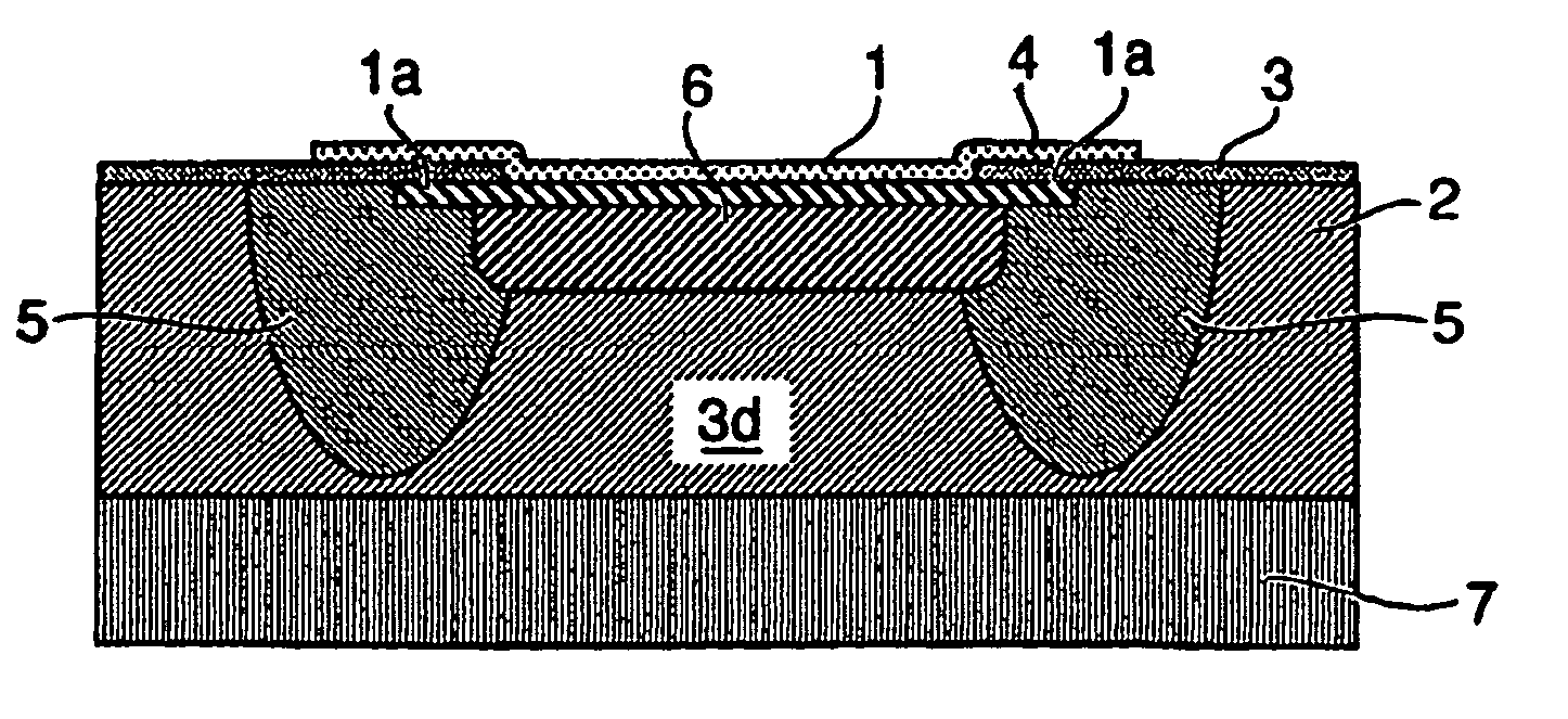
[0019]The fabrication of a p-substrate process will be described with reference to FIGS. 3a to 3d. It will of course be appreciated by one skilled in the art that the invention is equally applicable to an n-substrate process, in which case the conductivity types are reversed.

[0020]In FIG. 3a, a heavily doped n+ source and drain region 1 is diffused into a p-type epitaxial layer 2 in a conventional manner to form a pn junction. The epitaxial layer 2 is covered with an insulator / oxide layer 3 with an opening to receive a metal contact layer 4. This structure would normally break down at an unacceptably low voltage due to corner and edge avalanche effects at the junction of the n+ diffusion region 1 and the p-type layer 2.

[0021]In order to suppress breakdown of the n+ diffusion region 1, an n-well 5 is located at the edges 1a of the region 1 by a technique which per se is well known to one skilled in the art. However, even in the presence of the n-well 5, breakdown will eventually occu...


PUM

PropertyMeasurementUnit
voltageaaaaaaaaaa
voltagesaaaaaaaaaa
supply voltageaaaaaaaaaa

Abstract

A protection device provides to integrated circuits against high voltages. The diode includes a diode connected to provide a safe discharge path for the high voltage currents. The diode is configured so that in reverse bias breakdown occurs across an area portion of its active junction. The device can dissipate a large amount of ESD energy in a minimal area.

Description

BACKGROUND OF THE INVENTION[0001]1. Field of the Invention[0002]This invention relates to the field of electrostatic discharge (ESD) protection, and in particular of to an ESD protection diode.[0003]2. Description of Related Art[0004]Protection diodes are used to protect integrated circuits, particularly CMOS circuits, from damage caused by electrostatic discharge. A basic requirement of protection diodes is that the breakdown voltage be greater than the full worst case supply voltage applied to the circuit. For silicon integrated circuits, this voltage is, typically, below 10 Volts. The energy dissipated in a protection diode when it beaks down is related to the breakdown voltage. For example, the energy dissipated in a protection diode for a nominal 350V circuit will be approximately 50 times higher than for a nominal 5V circuit.[0005]There are many protection systems in use today. The most prevalent ones are similar to that shown in FIG. 1, for a p-substrate process. In FIG. 1, d...

Claims


Application Information

Patent Timeline
Patent Type & Authority Patents(United States)
IPC IPC(8): A61K31/353A61K31/375A61K31/7048A61K38/48H01L23/60H01L27/02H01L29/866H02H9/04
CPCA61K31/353A61K31/375A61K31/7048A61K38/4873H01L27/0255H01L29/866A61K2300/00H02H9/04H03K19/00
Inventor ORCHARD-WEBB, JONATHAN HARRY
Owner TELEDYNE DIGITAL IMAGING INC
Why Eureka
Try Eureka