Method and apparatus for nitride spacer etch process implementing in situ interferometry endpoint detection and non-interferometry endpoint monitoring

Inactive Publication Date: 2005-12-20
LAM RES CORP
View PDF16 Cites 18 Cited by
  • Summary
  • Abstract
  • Description
  • Claims
  • Application Information

AI Technical Summary

Benefits of technology

[0019]Other aspects and advantages of the invention will become apparent from the following detailed description, t

Problems solved by technology

However, this need is specifically more pronounced during the one step silicon nitride spacer etch process as the aggressive nature of the etch chemistry implemented inevitably results in gate oxide punch through leading to changes in gate oxide dimensions.
As is well known, changes to the gate oxide are disfavored since they modify the electrical conductivity of the gate oxide and thus the transistor.
Thus far, however, the OES method has proven to be less than reliable and efficient etch endpoint detection as it causes the overetching or underetching of the silicon nitride layer, rendering the outcome of the one-s

Method used


Image

  • Method and apparatus for nitride spacer etch process implementing in situ interferometry endpoint detection and non-interferometry endpoint monitoring
  • Method and apparatus for nitride spacer etch process implementing in situ interferometry endpoint detection and non-interferometry endpoint monitoring
  • Method and apparatus for nitride spacer etch process implementing in situ interferometry endpoint detection and non-interferometry endpoint monitoring

Examples


Example

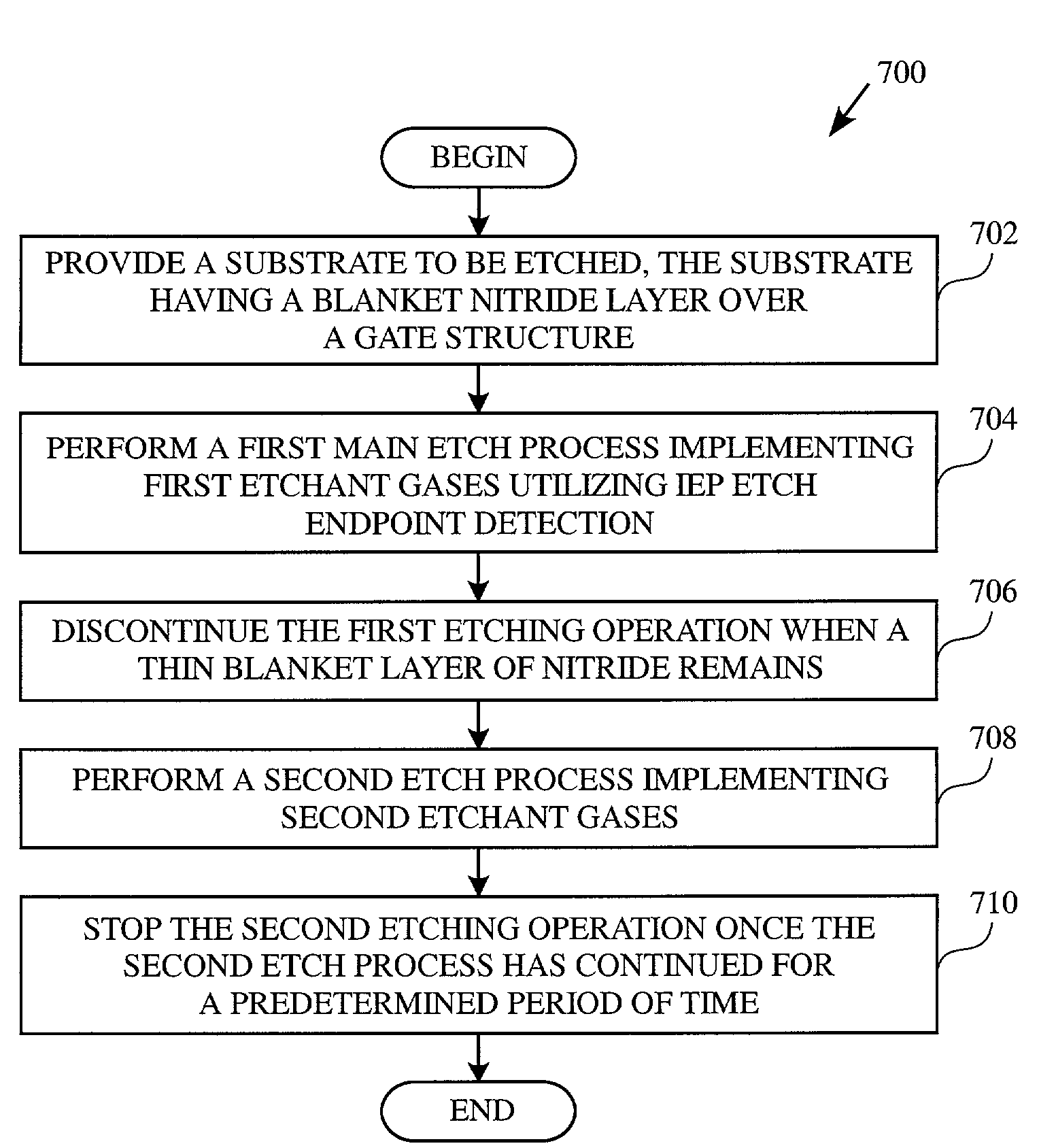
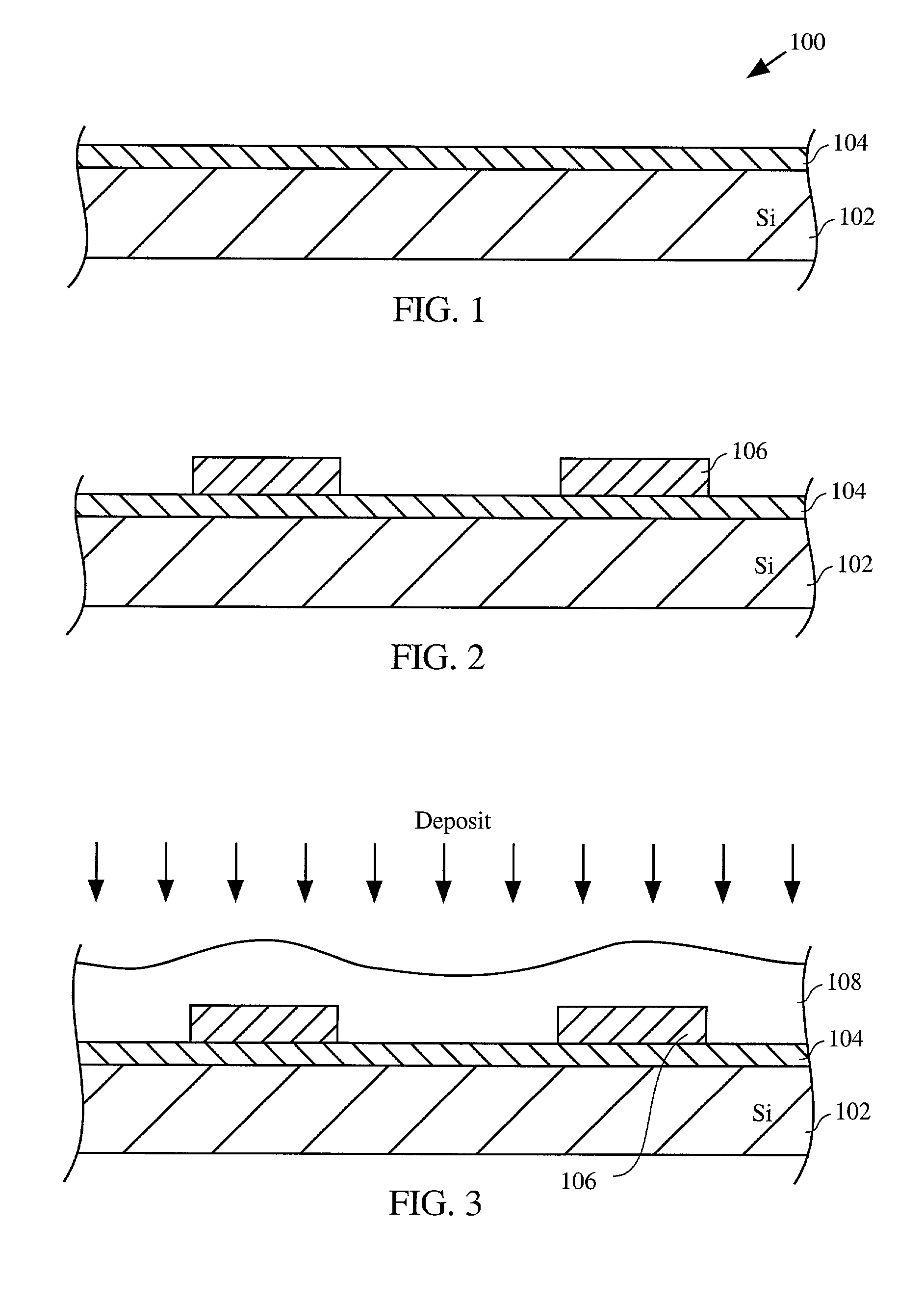
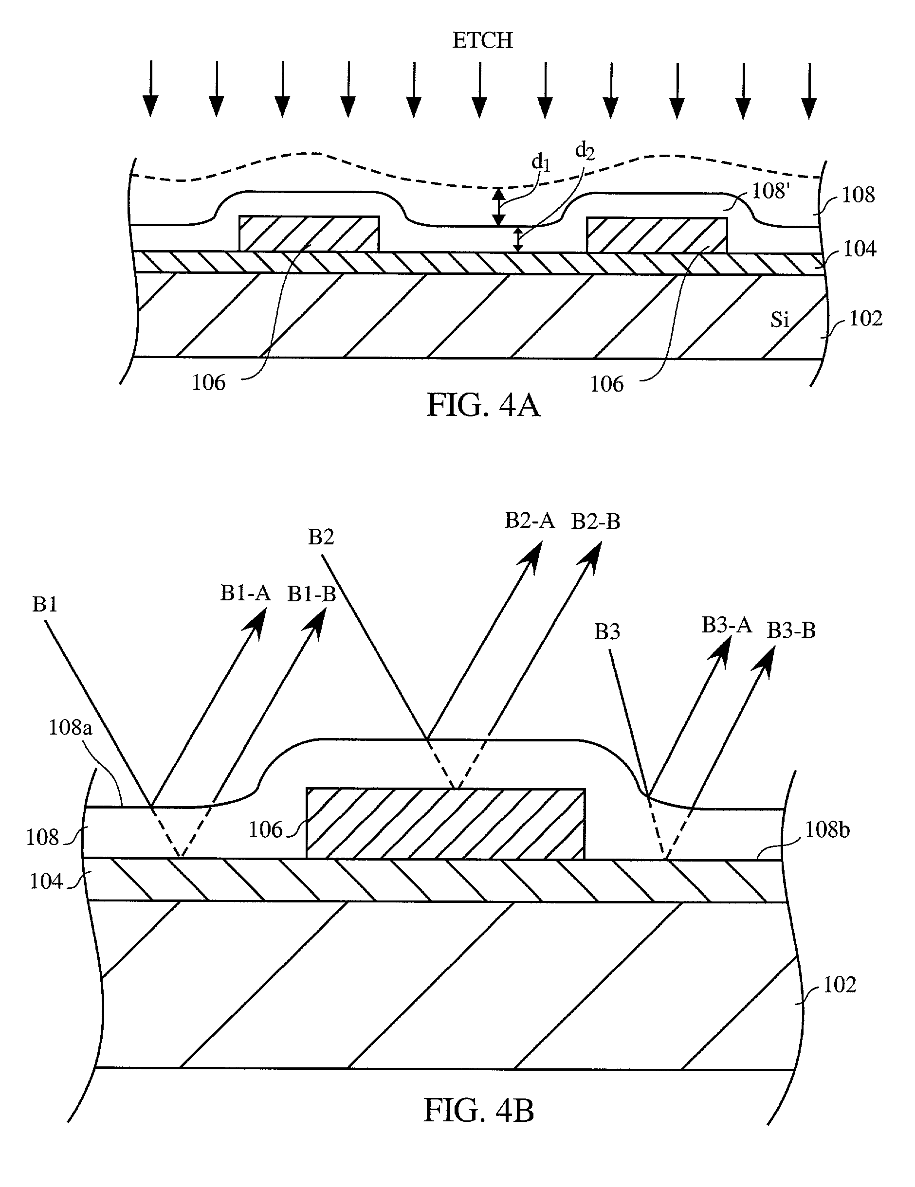
[0034]An invention for increasing wafer throughput through implementing an in-situ two-step etch process, is disclosed. Preferably, the in-situ two-step etch processes is used to etch a nitride (i.e., silicon nitride) spacer layer formed over a semiconductor substrate having a plurality of gate structures. During the first stage, an interferometry endpoint (IEP) system is implemented to detect the etch endpoint during a main etch process. Subsequently, an overetch process is performed. Preferably, the main etch process removes an etch depth of the nitride spacer layer leaving a thin layer of nitride. Thereafter, the remaining thin layer of nitride is removed in an overetch process. In one example, the etch depth is measured by implementing a distance between adjacent maximum or minimum fringes of a particular endpoint detection wavelength. In one embodiment, the thin layer of nitride is removed in the overetch process implementing the timed-etch method. In another example, the timed...


PUM


Abstract

A method for fabricating a spacer of a gate structure is provided. The method performing a first etch process implementing a first etchant gas. The first etch process is configured to implement an interferometry endpoint (IEP) detection method to detect a removal of a portion of a spacer layer having a specific thickness from over the surface of the substrate, thus leaving a thin spacer layer. The method further includes performing a second etch process for a predetermined period of time implementing a second etchant gas. The second etch process is configured to remove the thin spacer layer, leaving the spacer for the gate structure.

Description

BACKGROUND OF THE INVENTION[0001]1. Field of the Invention[0002]The present invention relates generally to the fabrication of semiconductor devices and, more particularly, to improving the fabrication of spacers by enhancing the etch endpoint detection of a nitride layer.[0003]2. Description of the Related Art[0004]As is well known, the semiconductor manufacturing process involves several stages during which millions of transistors including source / drain diffusion regions, a conductive polysilicon gate, and a dielectric gate oxide are fabricated on a single semiconductor chip. One of such fabrication stages is the silicon nitride spacer etch process during which a conformal layer of silicon nitride is deposited on a surface of the substrate having fabricated transistors. This silicon nitride layer is subsequently etched utilizing a plasma etch process, creating silicon nitride spacers alongside the polysilicon gates.[0005]As the demand for scaling down the integrated devices and thu...

Claims


Application Information

Patent Timeline
IPC IPC(8): H01J37/32H01L21/311H01L21/8234
CPCH01J37/3244H01L21/31116H01L21/823468
Inventor CHOU, WEN-BENCHENG, SHIH-YUANTU, WAYNE
Owner LAM RES CORP
Why Eureka
Try Eureka