
Planar lens and method for fabricating the same

a technology of plane lens and concave mold, which is applied in the field of plane lens, can solve the problems of limited concave mold processing method, limited cutting tools and diamond wheel curvature, and difficult to machine concave molds for lenses under 1 millimeter in diameter, and achieves easy manufacturing, good optical performance, and easy assembly of optical pickups.

Inactive Publication Date: 2006-02-07
SAMSUNG ELECTRONICS CO LTD
View PDF7 Cites 19 Cited by
  • Summary
  • Abstract
  • Description
  • Claims
  • Application Information

AI Technical Summary

Benefits of technology

[0016]The present invention provides a planar objective lens that is easy to manufacture, enables easy assembling of optical pickups, and has good optical performance, and a method for fabricating the planar objective lens.

Problems solved by technology

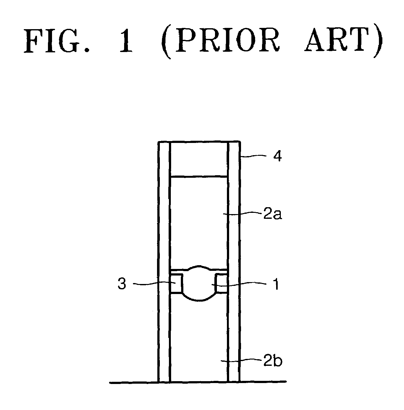
However, this mold processing method is limited as to processing a curved mold surface corresponding to a spherical or aspheric lens surface.
However, it is difficult to machine a concave mold for lenses under about 1 millimeter in diameter with the mechanical mold machining method, because cutting tools and the curvature of diamond wheels therefore are limited.
However, it is more difficult to manufacture and assemble smaller optical elements, especially with microlenses having a diameter of 1 mm or less because of difficulties in mold machining therefor, as described above.
Even though such microlenses of 1 mm or less in diameter can be manufactured, it is difficult to handle such a small microlens and to assemble an optical pickup with the microlens.
General objective lenses have two opposing surfaces that are spherical or aspheric and which protrude closer to an optical disc, compared to other adjacent optical elements, so they are likely to be abraded or damaged when collided with the optical disc.
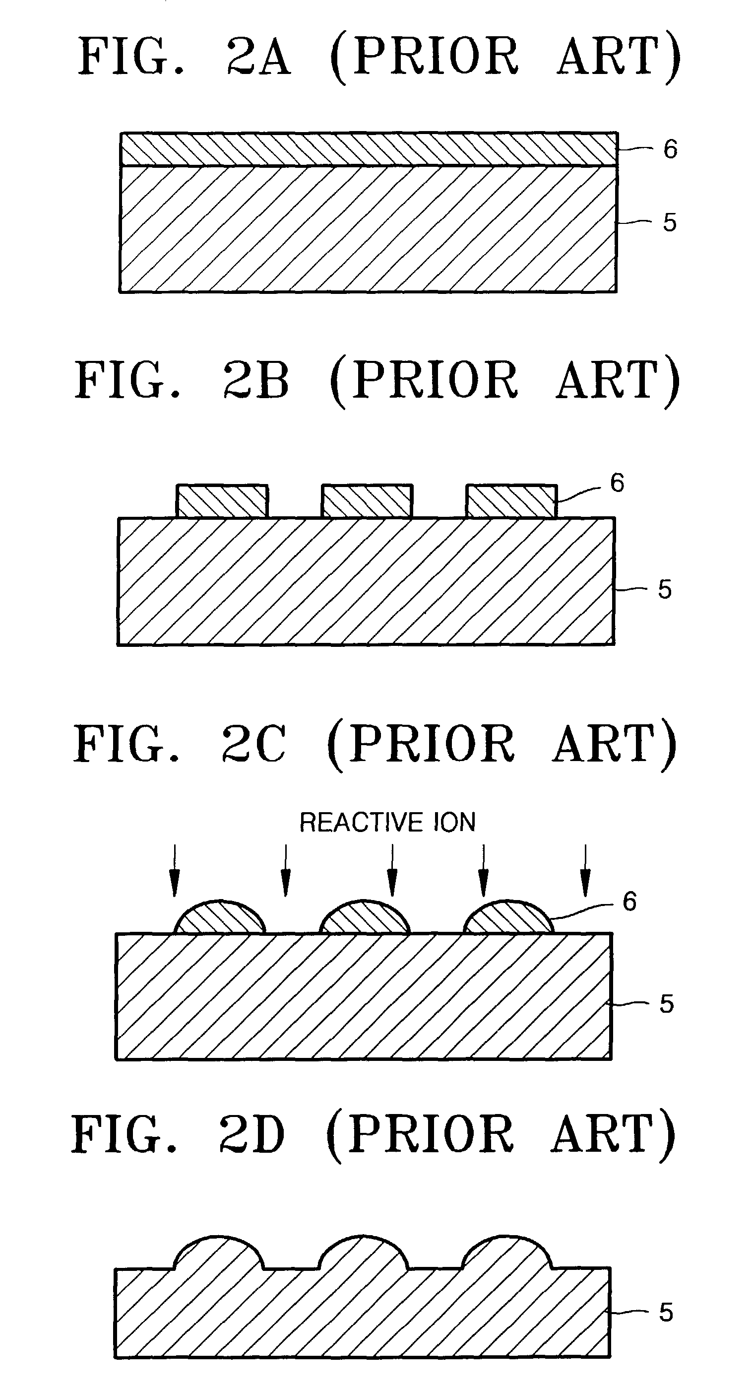
In this microlens array manufacturing method by plasma etching, it is difficult to uniformly deposit the photoresist to a sufficient thickness for an objective lens of appropriate thickness so that the sag height of the resulting microlens is limited.
In addition, since the hemispheric photoresist pattern formed by reflowing is directly transferred into a glass substrate, the method cannot be applied for general aspheric lenses excluding spherical lenses.
This method is suitable to manufacture single microlens but not for an array of multiple lenses.
Also, the thin film deposition technique, i.e., sputtering, used in the method takes a long duration for a lens layer having an appropriate thickness.
Furthermore, it is also time consuming to polish the deposited high refractive index material lens layer.

Method used


Image

  • Planar lens and method for fabricating the same
  • Planar lens and method for fabricating the same
  • Planar lens and method for fabricating the same

Examples


embodiment 1

[0042 of Lens Cavity Formation

[0043]Referring to FIG. 5A, the entire surface of a prepared substrate 12 is coated with photoresist 13 and subjected to light exposure through a mask 14 with a window 14a as a light transmission path. In this embodiment, positive photoresist is used so that a region to be etched is exposed to form the lens cavity 12a therebelow.

[0044]Next, the exposed region of the photoresist 13 is removed through a development process, as shown in FIG. 5B, to expose a cavity region of the substrate 12.

[0045]The exposed cavity region of the substrate 12, which is uncovered with the photoresist 13, is subjected to isotropic dry or wet etching so that the lens cavity 12a with a spherical bottom surface is formed, as shown in FIG. 5C.

[0046]After the remaining photoresist 13 is stripped away, as shown in FIG. 5D, and the process illustrated in FIG. 4C is performed.

embodiment 2

[0047 of Lens Cavity Formation

[0048]Referring to FIG. 6A, the entire surface of a prepared substrate 12 is coated with photoresist 13 and subject to light exposure through a gray scale mask 15 with a window 15 whose light transmittance locally varies. In this embodiment, positive photoresist is used so that a region to be etched is exposed to form the lens cavity 12a therebelow.

[0049]Since the window 15a of the gray scale mask 14 used in this embodiment has locally varying light transmittance, the amount of light radiated on the photoresist 13 during the exposure process through the window 15a is not uniform throughout the exposed region. The light transmittance of the window of the gray scale mask 14 needs to be appropriately controlled according to the curvature of a desired spherical or aspheric lens.

[0050]Next, a spherical or aspheric groove 13a is formed in the photoresist 13 through a development process, as shown in FIG. 6B.

[0051]Next, as shown in FIG. 6C, dry etching, for ex...


PUM

PropertyMeasurementUnit
Transparencyaaaaaaaaaa
Exposure limitaaaaaaaaaa

Abstract

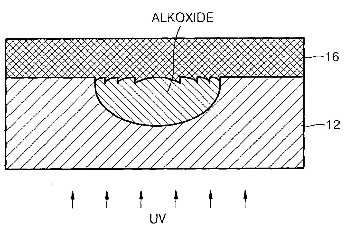
A planar lens capable of compensating for chromatic aberration and which is easy to manufacture and enables easy assembling of optical pickups and a method for fabricating the planar lens are provided. The planar lens includes a transparent substrate with a lens cavity in a surface of the transparent substrate, and a lens element formed in the lens cavity with a first refracting surface in contact with the bottom of the lens cavity and a second diffracting surface having a diffraction grating opposite to the first refracting surface.

Description

BACKGROUND OF THE INVENTION[0001]This application claims priority from Korean Patent Application No. 2002-70662, filed on Nov. 14, 2002, in the Korean Intellectual Property Office, the disclosure of which is incorporated herein in its entirety by reference.[0002]1. Field of the Invention[0003]The present invention relates to a planar lens and a method for fabricating the same, and more particularly, to an easy-to-fabricate planar objective lens capable of compensation of chromatic aberration, as an essential part of an optical pickup that is used in an optical disc drive (ODD) to write information in and / or reproduce information from an optical disc, such as a compact disc (CD) or a digital versatile disc (DVD), and an easy method for fabricating the planar microlens.[0004]2. Description of the Related Art[0005]Objective lenses are used to write information in an optical disc by focusing a laser beam emitted from a semiconductor laser used as a light source on a recording surface of...

Claims


Application Information

Patent Timeline
IPC IPC(8): B29D11/00G02B3/00B29C39/10B29L11/00G02B3/08G02B5/18G11B7/135G11B7/22
CPCG02B5/1814G02B3/08G02B3/00B29D11/00
Inventor LEE, MYUNG-BOKSOHN, JIN-SEUNGCHO, EUN-HYOUNGPARK, YOUNG-PIL
Owner SAMSUNG ELECTRONICS CO LTD
Learn More