Exposure method, exposure apparatus, and method of production of device

a technology of exposure apparatus and exposure method, which is applied in the direction of liquid fuel engine components, non-positive displacement fluid engines, photographic processes, etc., can solve the problems of two types of process errors, the degree of polishing change slightly, and the process error of the polished wafer, so as to prevent the accumulation of process errors and extreme deterioration of overlay accuracy. , the effect of high throughpu

Inactive Publication Date: 2006-02-21
NIKON CORP
View PDF5 Cites 24 Cited by
  • Summary
  • Abstract
  • Description
  • Claims
  • Application Information

AI Technical Summary

Benefits of technology

[0016]An object of the present invention is to provide a method of exposure by exposure apparatus designed for multiprocessing having a plurality of substrate stages or other processing systems, in particular a method of exposure able to prevent accumulation of process error and extreme deterioration in the overlay accuracy when exposing a substrate being processed after processing by a processing apparatus designed for multiprocessing and thereby produce high quality semiconductor chips with a high throughput.

Problems solved by technology

Sometimes, the degree of polishing changed slightly with each pad and two types of process error occurred in the polished wafers.
As a result, sometimes two types of process error occur.
When performing exposure by a conventional exposure apparatus for processing all wafers by the same wafer stage and alignment apparatus after such processing, there was the problem that the overlay accuracy at the time of exposure fell.
Further, in such a case, in the final analysis, only practical processing to try to reduce the process error itself in the prior step was possible.
On the other hand, in recently proposed exposure apparatuses provided with two substrate stages an explained above, the exposure apparatus itself generated process error corresponding to the number of the processing systems, that is, process error of the two substrate stages themselves like other processing apparatuses designed for multiprocessing.
Therefore, the situation had arisen that when such an exposure apparatus processed wafers etc. after processing by such an apparatus designed for multiprocessing, wafers having two typos of process error were exposed by an exposure apparatus having a further two types of process error, so the process error grew ad therefore the overlay accuracy greatly deteriorated.

Method used


Image

  • Exposure method, exposure apparatus, and method of production of device
  • Exposure method, exposure apparatus, and method of production of device
  • Exposure method, exposure apparatus, and method of production of device

Examples


Embodiment Construction

[0064]An embodiment of the present invention will be explained first with reference to FIG. 1 to FIG. 5.

[0065]In the present embodiment, the present invention will be explained illustrating part of the process of wafer processing in a production line of semiconductor integrated circuits.

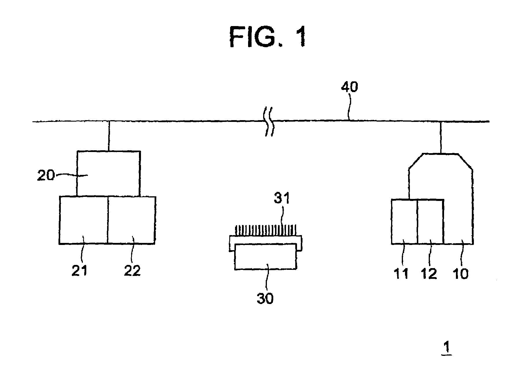
[0066]FIG. 1 is a view schematically showing part of the production line.

[0067]The semiconductor integrated circuit production line 1 has an exposure apparatus 10, a wafer processing apparatus 20, and a communications line 40.

[0068]First, the general configuration of the semiconductor integrated circuit production line 1 will be explained.

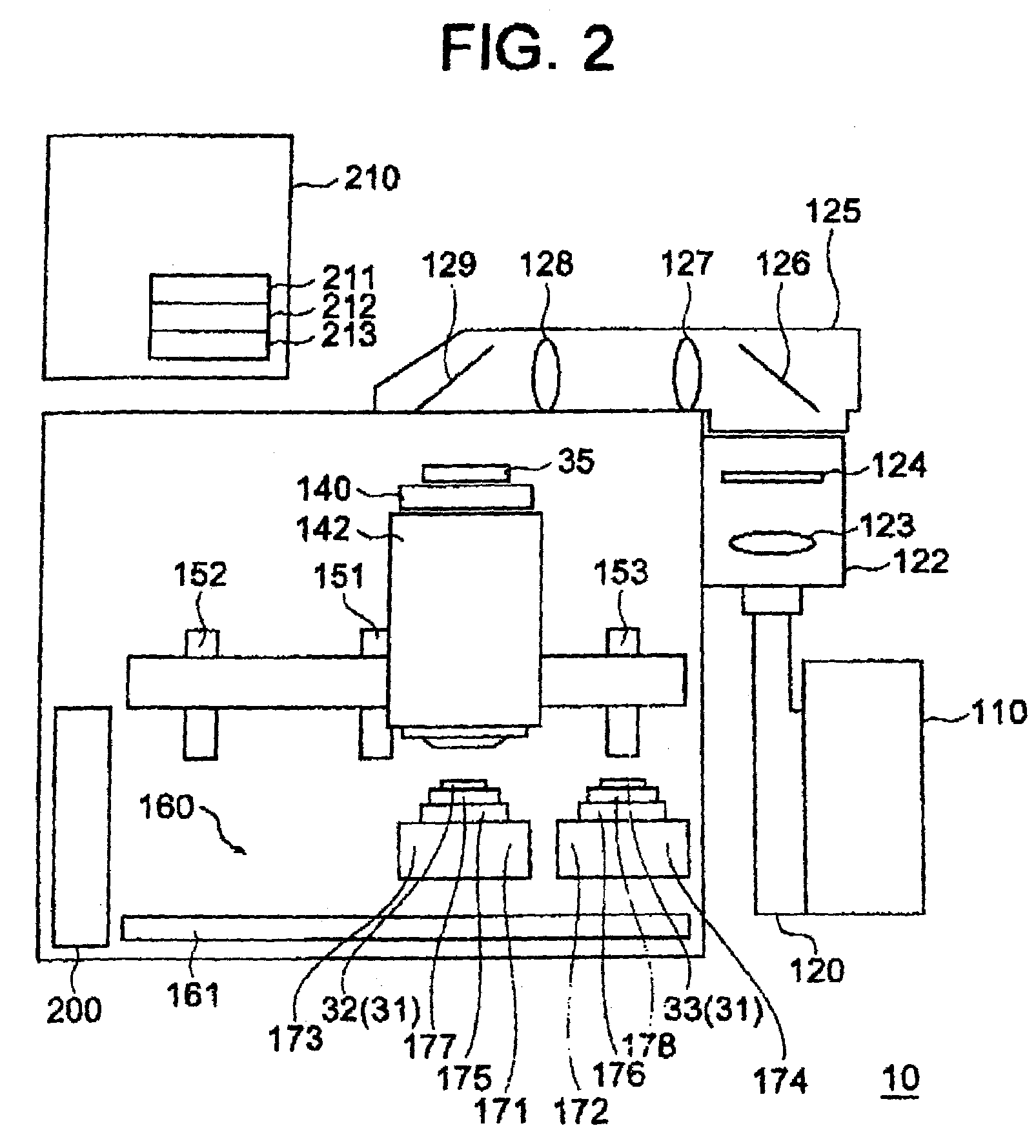
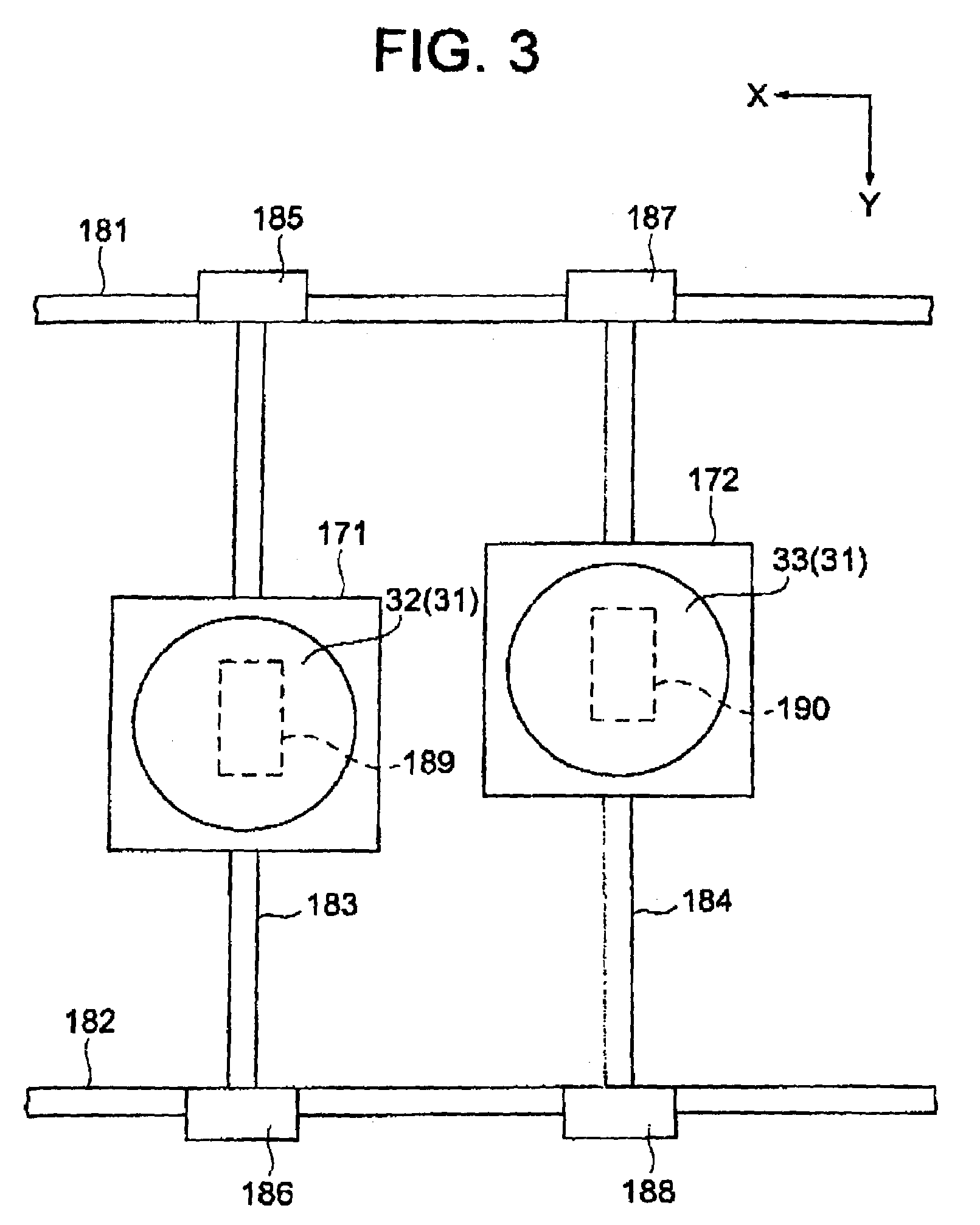
[0069]The exposure apparatus 10 is an apparatus for transferring a pattern drawn on a reticle serving as a mask through a projection optical system on to a wafer coated with a photosensitizing material (sensitive substrate). In the prevent embodiment, it is a step-and-scan type projection exposure apparatus.

[0070]The exposure apparatus 10 is an apparatus designed fo...


PUM

PropertyMeasurementUnit
speedaaaaaaaaaa
photosensitiveaaaaaaaaaa
mechanical structureaaaaaaaaaa

Abstract

An exposure method for preventing accumulation of process error for substrates processed by an apparatus designed for multiprocessing and producing high quality semiconductor chips. A semiconductor integrated circuit production line polishes wafers of individual lots at a first processing system and second processing system of a CMP system two at a time. Wafer processing information indicating at which processing system of the first processing system and second processing system each wafer has been processed is transmitted through a communication line to a later processing apparatus including an exposure apparatus. The wafers of a lot loaded in the exposure apparatus are allocated to a plurality of processing systems of the exposure apparatus so that wafers processed by the same processing system are processed by the same processing system among the two processing systems of the exposure apparatus and are exposed at those processing systems.

Description

BACKGROUND OF THE INVENTION[0001]1. Field of the Invention[0002]The present invention relates to an exposure method and exposure apparatus for producing a semiconductor integrated circuit, a liquid crystal display element, a thin film magnetic head, or another micro device or other semiconductor chip, a photomask, a reticle, etc. using photolithography, more particularly relates to an exposure method using an exposure apparatus able to perform processing in parallel on a plurality of wafers or other substrates, an exposure apparatus for the same, and a method of production of a device using such an exposure method and exposure apparatus.[0003]2. Description of the Related Art[0004]In the process of production of a wafer when producing a semiconductor integrated circuit etc., a desired circuit is formed on a silicon or other wafer by repetition of processing such as oxidation, thin film formation, doping, resist processing, exposure, etching, cleaning, chemical mechanical polishing (...

Claims


Application Information

Patent Timeline
Patent Type & Authority Patents(United States)
IPC IPC(8): B32B15/01F03B3/12G03F7/20G03F7/207G03F9/00H01L21/027
CPCG03F7/70525G03F7/70541G03F7/70633G03F7/70991Y10T428/12937Y10T428/12931Y10T428/12944
Inventor IRIE, NOBUYUKI
Owner NIKON CORP
Why Eureka
Try Eureka