Method and apparatus for monitoring and adjusting chamber impedance

a technology of impedance monitoring and impedance adjustment, applied in the field of integrated circuit fabrication, can solve the problems of substantially interfering with film deposition and increasing the problem of arcing, and achieve the effect of minimizing phase interference and greatly reducing the potential for arcing

Inactive Publication Date: 2006-02-28
APPLIED MATERIALS INC
View PDF40 Cites 104 Cited by
  • Summary
  • Abstract
  • Description
  • Claims
  • Application Information

AI Technical Summary

Benefits of technology

[0013]The present invention provides an improved method and apparatus for depositing CVD films on a substrate. The apparatus employs mixed frequency RF power and includes a gas distribution manifold with conical holes. The potential for arcing is greatly reduced by connecting the low frequency RF power source to an electrode embedded in the substrate holder and connecting the high frequency RF power source to the gas distribution manifold, which also functions as an electrode. An independent matching network decouples the low frequency waveform from the high frequency waveform to minimize phase interferences between the waveforms.
[0014]These features combine to allow deposition processes to proceed at conditions that were unattainable in prior substrate processing chambers and also enable the substrate processing apparatus of the present invention to be usable in sub-0.35 μm deposition processes including 0.25 and 0.18 μm processes.
[0016]In one preferred embodiment of the method of the present invention, a silicon nitride film is deposited. A process gas including silane, ammonia and molecular nitrogen is introduced through a gas distribution manifold having conical holes and a plasma is formed from the process gas using mixed frequency RF power. The high frequency (HF) component is applied to the gas distribution manifold while the low frequency (LF) component is applied to a bottom electrode. It has been demonstrated that silicon nitride films deposited according to this embodiment under low temperature processing conditions can have a wet etch rate (WER) as low as 170 Å / min while retaining excellent step coverage properties at aspect ratios of 2:1 or higher. It has also been demonstrated that silicon nitride films deposited according to this embodiment under high temperature processing conditions (above 580° C.) can have a WER of 15 Å / min or less.
[0017]In part, the excellent physical characteristics of these silicon nitride films are achieved because the films can be deposited at pressure and RF power levels that were previously not possible in other chambers. For example, in a more preferred embodiment, the ratio of LF power to total RF power is greater than 50%, while in another preferred embodiment, the silicon nitride deposition sequence takes place at a pressure between 2 and 5 torr. The physical characteristics are also achieved in part through the use of the conical holes, which in turn increases the plasma density and ionization efficiency of the created plasma thus allowing an increased amount of N2 as compared with NH3 to be used in the film's process gas. Reduced NH3 content in the process gas results in less hydrogen in the film and a lower WER.
[0018]In another embodiment, a bipolar low frequency asymmetric RF waveform, also referred to as a triangular or sawtooth waveform, is employed to control ion bombardment. Such an asymmetric RF waveform enhances ion bombardment at the substrate while hindering the formation of harmonics, which the present inventors have discovered can provoke plasma sheath instabilities.

Problems solved by technology

In these experiments, it was found that the arcing problem was further increased to the point that it substantially interfered with film deposition.

Method used


Image

  • Method and apparatus for monitoring and adjusting chamber impedance
  • Method and apparatus for monitoring and adjusting chamber impedance
  • Method and apparatus for monitoring and adjusting chamber impedance

Examples


invention example 1

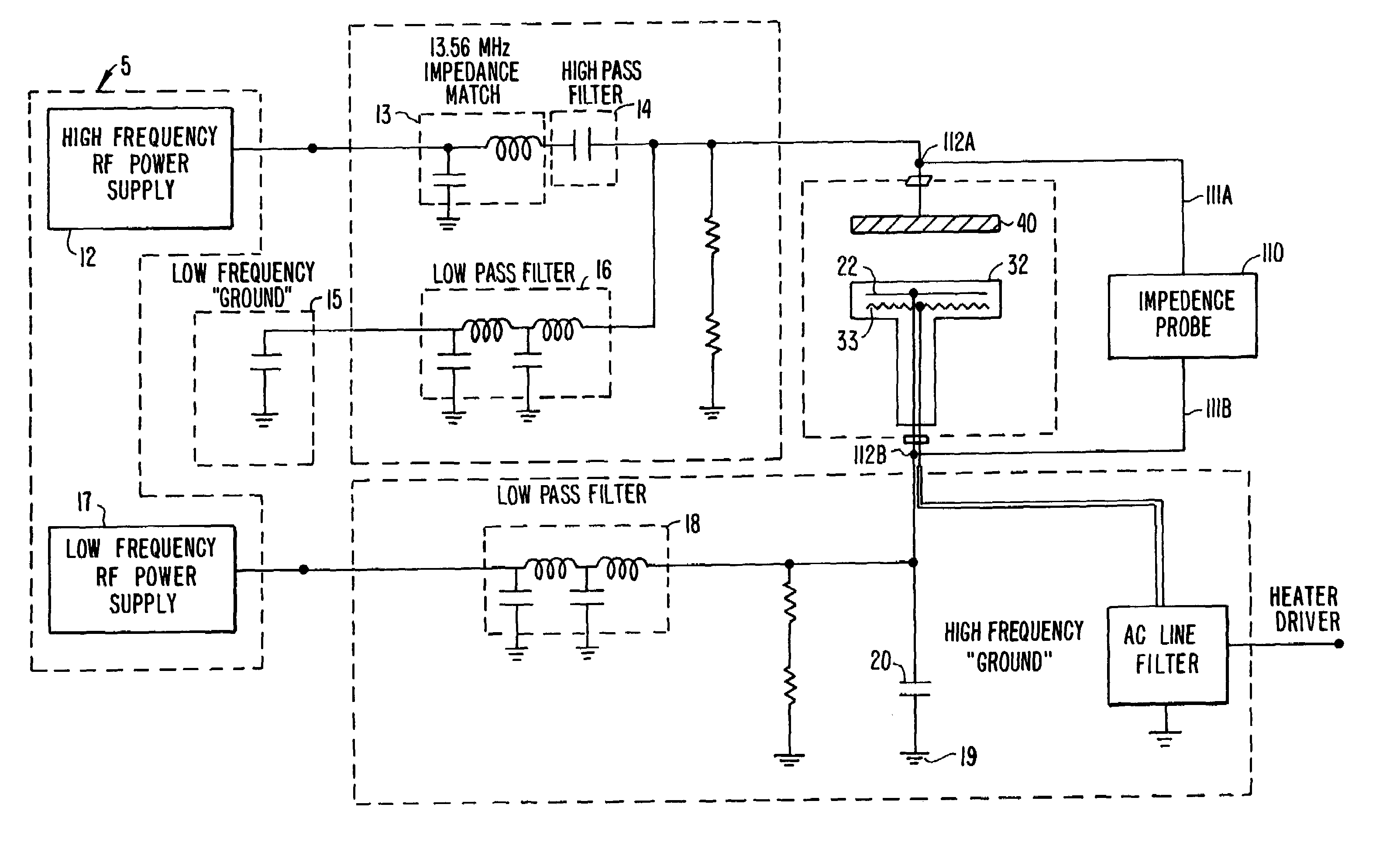
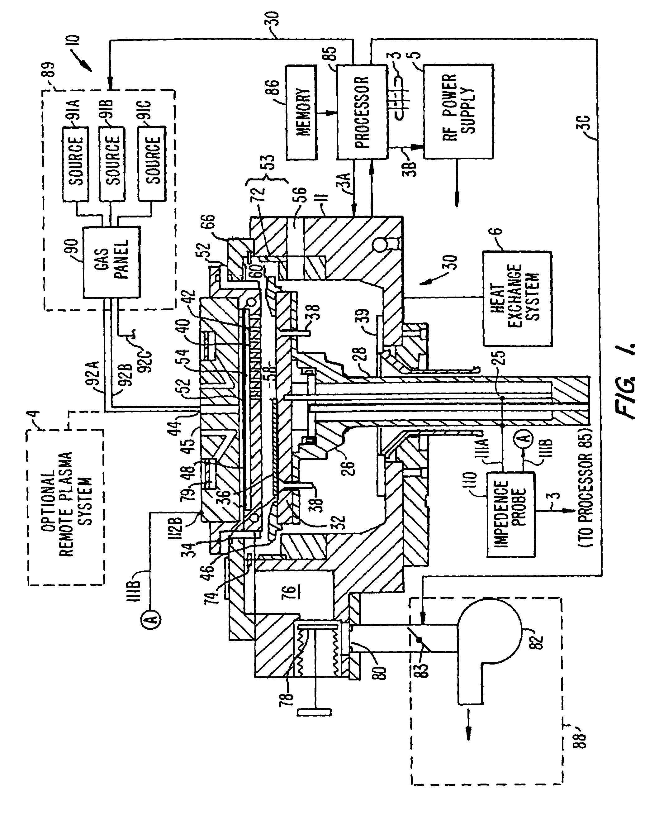
[0113]This example was undertaken using a chemical vapor deposition chamber, and in particular, a “D×Z” plasma reactor fabricated and sold by Applied Materials, Inc., Santa Clara, Calif. The reactor was modified to include both a conical holes gas distribution manifold and a ceramic substrate holder in accordance to the present invention and as shown in FIG. 1. High frequency RF power was provided to the gas distribution manifold and low frequency RF power was provided to RF electrode 22 embedded in the ceramic substrate holder. The substrate holder held a wafer positioned 600 mil from the gas distribution manifold during processing.

[0114]The reactor was pumped down to a pressure of 0.1 torr at a temperature of 400° C. and then stabilized at 2.5 torr with process gas flow rates of 65 sccm of silane, 130 sccm of ammonia, and 1450 sccm of nitrogen. Then 160 W of high frequency RF power (13.56 MHz) was applied to the gas distribution manifold and 135 W of low frequency RF power (sinuso...

invention example 2

[0115]This example was undertaken using the modified chemical vapor deposition chamber of Example 1. The substrate holder held a wafer positioned 485 mil from the gas distribution manifold during processing.

[0116]The reactor was pumped down to a pressure of 0.1 torr at a temperature of 400° C. and then stabilized at 4.0 torr with process gas flow rates of 210 sccm of silane, 1200 sccm of ammonia, and 600 sccm of nitrogen. Then 250 W of high frequency RF power (13.56 MHz) was applied to the gas distribution manifold and 250 W of low frequency RF power (sinusoidal waveform, 350 kHz) was applied to the ceramic substrate holder. The silicon nitride film was deposited at 5525 Å / min. The deposited film had a refractive index of 2.0 and a stress of −1.6×10⁹ dynes / cm2.

[0117]The deposited film also had a WER of 335 Å / min. Etching of the deposited film to remove about 250 Å of the silicon nitride from the field left a substantial amount of the silicon nitride in the bottom corners of the vias...

invention example 3

[0118]This example was undertaken using the modified chemical vapor deposition chamber of Example 1. The substrate holder held a wafer positioned 490 mil from the gas distribution manifold during processing.

[0119]The reactor was pumped down to a pressure of 0.1 torr at a temperature of 400° C. and then stabilized at 4.0 torr with process gas flow rates of 200 sccm of silane, 1200 sccm of ammonia, and 600 sccm of nitrogen. Then 170 W of high frequency RF power (13.56 MHz) was applied to the gas distribution manifold and 250 W of low frequency RF power (sinusoidal waveform, 350 kHz) was applied to the ceramic substrate holder. The silicon nitride film was deposited at 4625 Å / min. The deposited film had a refractive index of 2.0 and a stress of −2×10⁹ dynes / cm2.

[0120]The deposited film had a WER of 293 Å / min. Comparison of these results to Example 2 demonstrates an inverse relationship between the ratio of low frequency RF power to total RF power and WER when varying the high frequency...


PUM

PropertyMeasurementUnit
temperatureaaaaaaaaaa
pressureaaaaaaaaaa

Abstract

A substrate processing system that includes a deposition chamber having a reaction zone, a substrate holder that positions a substrate in the reaction zone, a gas distribution system that includes a gas inlet manifold for supplying one or more process gases to said reaction zone, a plasma power source for forming a plasma from a process gas introduced into the reaction zone of the deposition chamber and an impedance monitor that is electrically coupled to the deposition chamber to measure an impedance level of the plasma. In a preferred embodiment, the substrate holder is a first electrode and the gas inlet manifold is a second electrode and RF power is supplied by the plasma power source to either the first or second electrodes to form the plasma. In another preferred embodiment, the processing system further includes a computer processor that is communicatively coupled to the impedance monitor and to other control systems of the processing system so that the computer processor can adjust the impedance of the deposition chamber during the course of an extended wafer run if the impedance drifts outside of a predetermined tolerance range.

Description

CROSS-REFERENCE TO RELATED APPLICATIONS[0001]This application is related to concurrently filed and commonly assigned patent application Ser. No. 08 / 980,520 entitled “MIXED FREQUENCY CVD PROCESS AND APPARATUS,” having Sébastien Raoux, Mandar Mudholkar, William N. Taylor, Mark Fodor, Judy Huang, David Silvetti, David Cheung and Kevin Fairbairn listed as co-inventors; and to concurrently filed and commonly assigned patent application Ser. No. 08 / 982,121 entitled “SUBSTRATE PROCESSING CHAMBER WITH TUNABLE IMPEDANCE,” having Sébastien Raoux, Mandar Mudholkar and William N. Taylor listed as co-inventors; and to concurrently filed and commonly assigned patent application Ser. No. 08 / 982,252 entitled “USE OF AN ASYMMETRIC WAVEFORM TO CONTROL ION BOMBARDMENT DURING SUBSTRATE PROCESSING,” having Sébastien Raoux and Mandar Mudholkar listed as co-inventors. This application is also related to U.S. patent application entitled “A HIGH TEMPERATURE CERAMIC HEATER ASSEMBLY WITH RF CAPABILITY AND REL...

Claims


Application Information

Patent Timeline
Patent Type & Authority Patents(United States)
IPC IPC(8): C23C16/509H01L21/306C23F1/00H05H1/46C23C16/44C23C16/455C23C16/52C23C16/54H01J37/32H01L21/31
CPCC23C16/45565H01J37/32174C23C16/52C23C16/5096
Inventor RAOUX, SEBASTIENMUDHOLKAR, MANDARTAYLOR, WILLIAM N.
Owner APPLIED MATERIALS INC
Why Eureka
Try Eureka