Organic light-emitting devices

a light-emitting device and organic technology, applied in the direction of instruments, discharge tubes luminescnet screens, natural mineral layered products, etc., can solve the problems of irregular thickness of the resulting organic layer, defects formation of holes in the organic layer, so as to limit the current flow

Inactive Publication Date: 2006-02-28
CAMBRIDGE DISPLAY TECH LTD
View PDF24 Cites 35 Cited by
  • Summary
  • Abstract
  • Description
  • Claims
  • Application Information

AI Technical Summary

Benefits of technology

[0018]According to a first aspect of the present invention there is provided an organic light-emitting device comprising a light-emissive organic layer interposed between first and second electrodes for injecting charge carriers into the light-emissive organic layer and means for limiting the current flow through any conductive defect in said light-emissive organic layer. In contrast to the “burn out” technique referred to above, the incorporation into the device of means for limiting the current flow through any conductive defect in the light-emissive layer prevents any current anomalies arising during the lifetime of the device from rising to such a level as to significantly affect device operation in the manner described above.
[0019]Preferably the means are incorporated into at least one of said first and second electrodes of the device. In particular, the electrode may comprise a plurality of layers including a first electrode layer adjacent the surface of the light-emissive organic layer remote from the other of the first and second electrodes and having a resistance selected such that it is not too high to cause a significant increase in the drive voltage of the device, yet high enough to prevent excessive currents at any conductive defect in said light-emissive organic layer.
[0020]According to one embodiment of the invention, the first electrode layer may comprise a high-resistance material selected from the group consisting of a mixture of a semiconductor material with an insulator material, a mixture of a semiconductor material with a conductor material and a mixture of an insulator material with a conductor material. The use of a layer of the above-mentioned mixtures of materials as the high resistance electrode layer has the advantage that the resistance of the high resistance electrode layer can be easily adjusted to the desired value by simply adjusting the relative proportions of the components of the mixture accordingly.

Problems solved by technology

If the organic material is contaminated with particles having a size of the order of the thickness of the organic layer, not only will these particles themselves give rise to defects in the resulting organic layer, their presence disrupts the movement of the fluid organic material over the surface of the first electrode layer leading to variations in the thickness of the resulting organic layer about the particle, and in the worst case leading to the formation of holes in the organic layer through which the underlying layer (electrode layer) is exposed.
Defects in the organic layer can also be caused by, for example, inherently poor film-forming properties of the organic material, or by physical damage to the organic layer after deposition.
This leads, inter alia, to problems of device reproducibility and is a particular problem in dot matrix devices since it provides alternative current paths that lead to the wrong pixels being lit.
However, a typical clean room has particle size levels specified down to 300 nm and the organic material is only typically filtered to about 450 nm, since the elimination of particles having smaller sizes requires great expense.
The light-emissive organic material will therefore often still be contaminated with particles having a size of the order of the thickness of the organic layer to be deposited, which will, as mentioned above, lead to defects in the resulting organic layer.
Furthermore, even if the contamination by such large particles could be completely eliminated, defects can still arise during the manufacturing process as a result, for example, of inherently poor film-forming properties of the organic material itself, or due to physical damage inadvertently inflicted on the organic layer after deposition.
However, this technique is not applicable to all defect particles and cannot be used to resolve the problem of large shorts.
Moreover, it does not necessarily deal with problems that may manifest themselves in the lifetime of the device.
High resolution is readily achieved and is principally limited only by the overlap area of the cathode and the anode and thus by the size of the cathode and the anode.
However, shadow masking may not be desirable for various reasons.
In particular, there are significant constraints on the use of shadow masks when displays of large area and / or high resolution are required.
Maintaining the desired electrical and light output characteristic of the pixels in an OLED display when lithographic processes are used to fabricate the electrode patterns, in particular where those patterns are on top of the at least one organic layer, is not trivial owing to the risk of the lithographic processes modifying and potentially damaging the organic layer / electrode interfaces and the vicinity.
Such damage during lithography may originate from the photoresist, the developers, the etching processes (both dry and wet, negative and positive techniques and etch and lift-off) or the solvents used.
Organic electroluminescent and charge transporting materials would normally be damaged, modified and / or etched very rapidly in such dry etching / ashing processes if directly exposed to the plasma.

Method used


Image

  • Organic light-emitting devices
  • Organic light-emitting devices
  • Organic light-emitting devices

Examples


Embodiment Construction

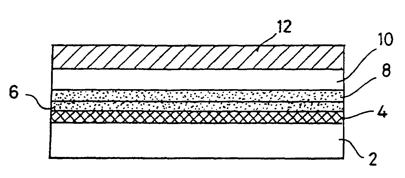
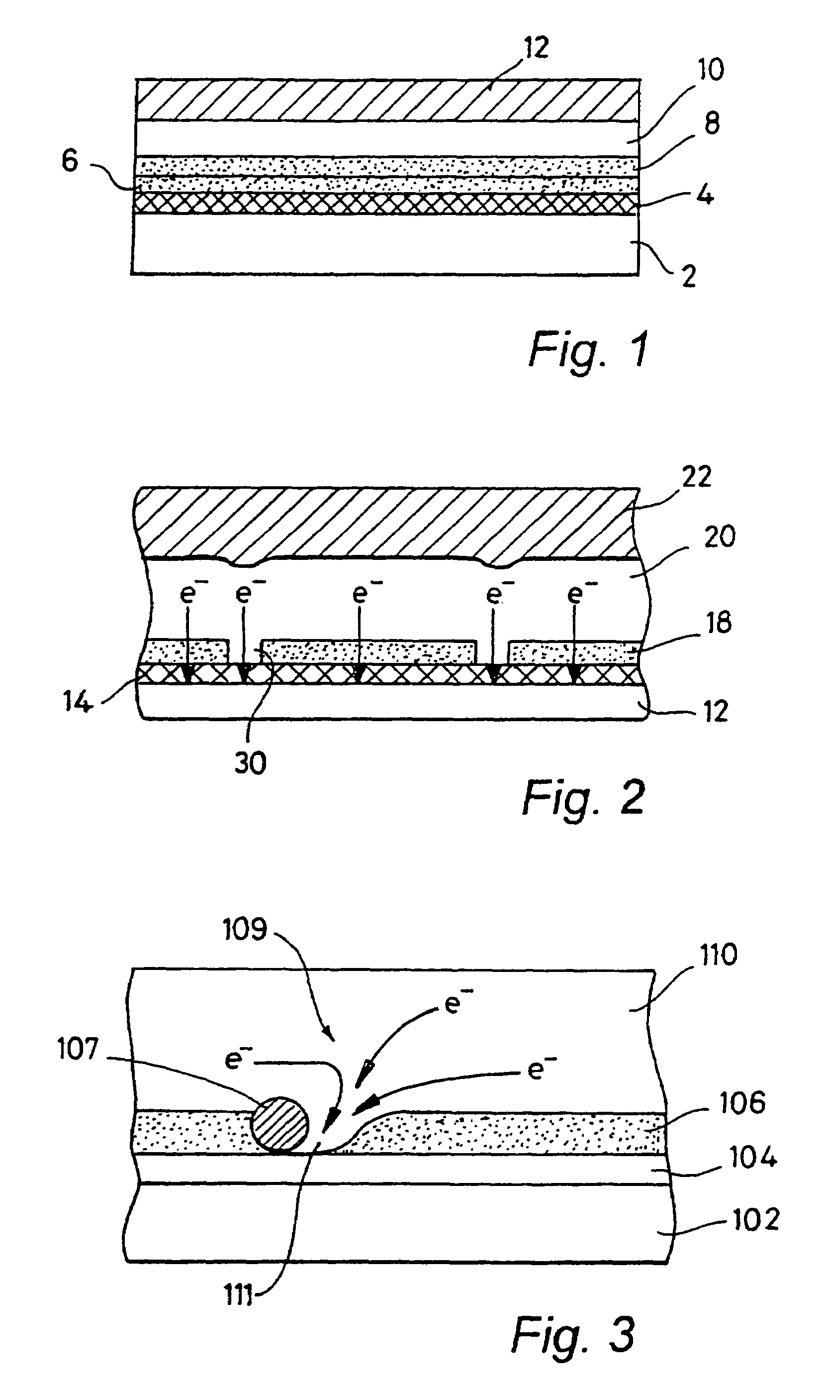
[0070]FIG. 1 shows an OLED according to a first embodiment of the present invention.

[0071]A glass substrate 2 having a thickness of 1.1 mm is coated with a layer 4 of indium tin oxide (ITO) with a sheet resistance of 15 Ohms / sq. to a thickness of 150 nm. Although not shown in FIG. 1, this is patterned to form a series of parallel strips using, for example, standard photolithographic and etch processes. A layer 6 of polyethylenedioxythiophene doped with polystyrene sulphonic acid (PEDT:PSS) is spun on the anode layer 4 and subsequently baked at 150° C. to remove water leaving a layer of 50 nm thickness. A layer 8 of a light-emissive polymer such as a blend of 5% poly(2,7-(9,9,di-n-octylfluorene)-3,6-(benzothiadiazole) with 95% poly(2,7-(9,9-di-n-octylfluorene) (5BTF8) doped with poly(2,7-(9,9-di-n-octylfluorene)-(1,4-phenylene-((1,4-phenylene-((4-secbutylphenyl)imino)-1,4-phenylene)) (TFB) is then spun on to the layer 6 of PEDT:PSS to a thickness of 75 nm. A cathode layer 10 is then ...


PUM

PropertyMeasurementUnit
thicknessaaaaaaaaaa
sizesaaaaaaaaaa
particle sizeaaaaaaaaaa

Abstract

An organic light-emitting device comprising a light-emissive organic layer (8) interposed between first (4) and second (12) electrodes for injecting charge carriers into the light-emissive organic layer (8), at least one of said first and second electrodes comprising a plurality of layers including a first electrode layer (10) having a high resistance adjacent the surface of the light-emissive organic layer (8) remote from the other of the first and second electrodes, said first electrode layer (10) comprising a high-resistance material selected from the group consisting of a mixture of a semiconductor material with an insulator material, a mixture of a semiconductor material with a conductor material and a mixture of an insulator material with a conductor material.

Description

FIELD OF THE INVENTION[0001]This invention relates to organic light-emitting devices (OLEDs) and a method for improving the uniformity of current density of OLEDs having a light-emissive organic layer containing intrinsic defects.[0002]The present invention also relates to organic light-emissive devices having patterned electrodes.BACKGROUND TO THE INVENTION[0003]Organic light-emitting devices such as described in U.S. Pat. No. 5,247,190 or in U.S. Pat. No. 4,539,507, the contents of which are incorporated herein by reference, have great potential for use in various display applications. According to one method, an OLED is fabricated by coating a glass or plastic substrate with a transparent first electrode (anode) such as indium tin oxide (ITO). At least one layer of a thin film of an electroluminescent organic material is then deposited prior to a final layer which is a film of a second electrode (cathode) which is typically a metal or alloy.[0004]In many practical applications, t...

Claims


Application Information

Patent Timeline
Patent Type & Authority Patents(United States)
IPC IPC(8): H05B33/14H05B33/26H01L51/50H01L51/52H05B33/22
CPCH01L51/5203Y10S428/917H01L2251/5361H10K59/805H10K50/16H10K50/805H10K50/11
Inventor CARTER, JULIAN CHARLESBURROUGHES, JEREMY HENLEYHEEKS, STEPHEN KARL
Owner CAMBRIDGE DISPLAY TECH LTD
Why Eureka
Try Eureka