Silicon carbide and related wide-bandgap transistors on semi-insulating epitaxy for high-speed, high-power applications

a wide-bandgap transistor and semi-insulating epitaxy technology, applied in the field of advanced microelectronic devices, can solve problems such as inability to use current implant technology in si

Inactive Publication Date: 2006-03-07
MISSISSIPPI STATE UNIVERSITY
View PDF10 Cites 41 Cited by
  • Summary
  • Abstract
  • Description
  • Claims
  • Application Information

AI Technical Summary

Benefits of technology

[0007]It is an advantage of the present invention to use lower-cost, conducting SiC subst...

Problems solved by technology

This is not feasible in SiC...

Method used


Image

  • Silicon carbide and related wide-bandgap transistors on semi-insulating epitaxy for high-speed, high-power applications
  • Silicon carbide and related wide-bandgap transistors on semi-insulating epitaxy for high-speed, high-power applications
  • Silicon carbide and related wide-bandgap transistors on semi-insulating epitaxy for high-speed, high-power applications

Examples


Embodiment Construction

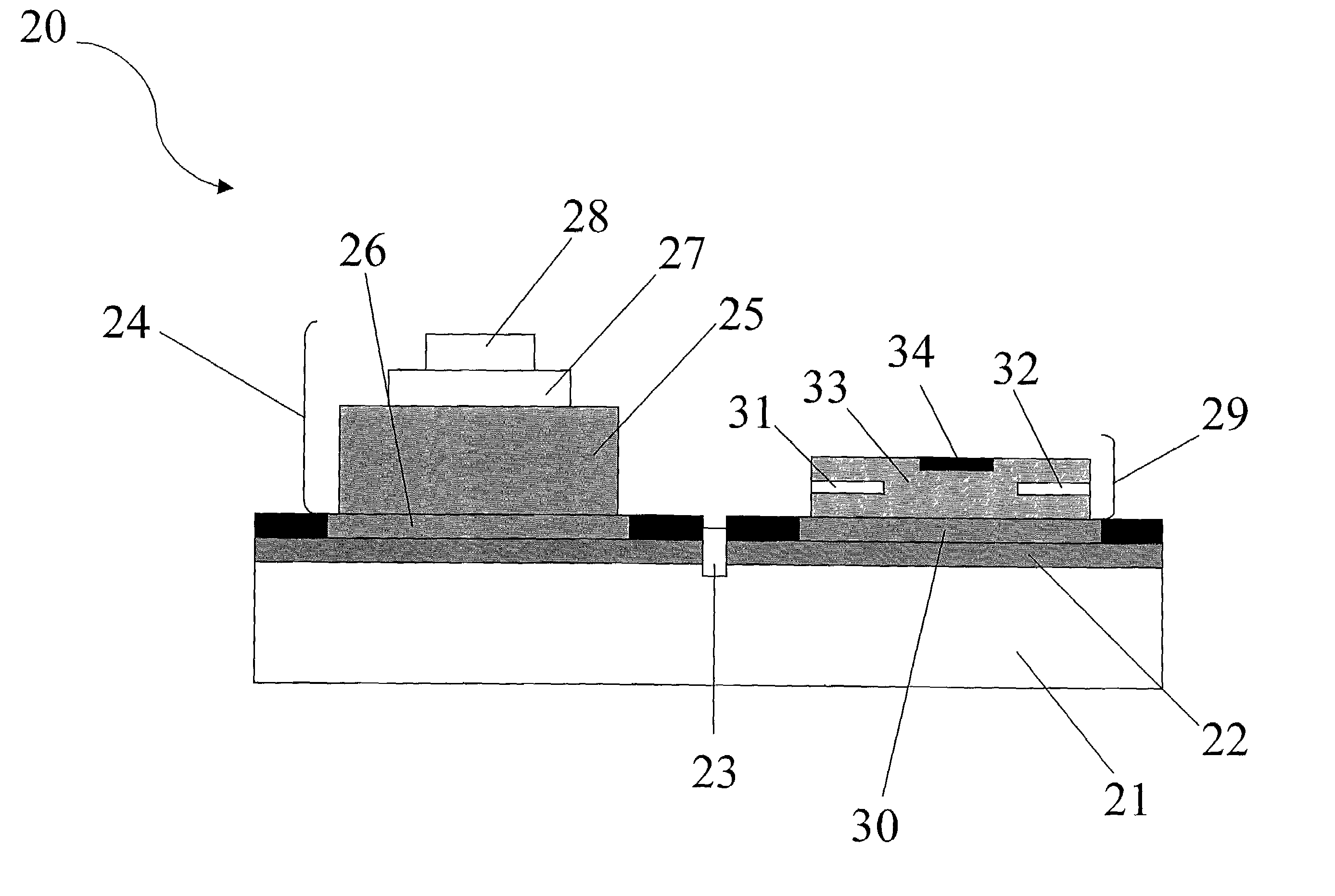
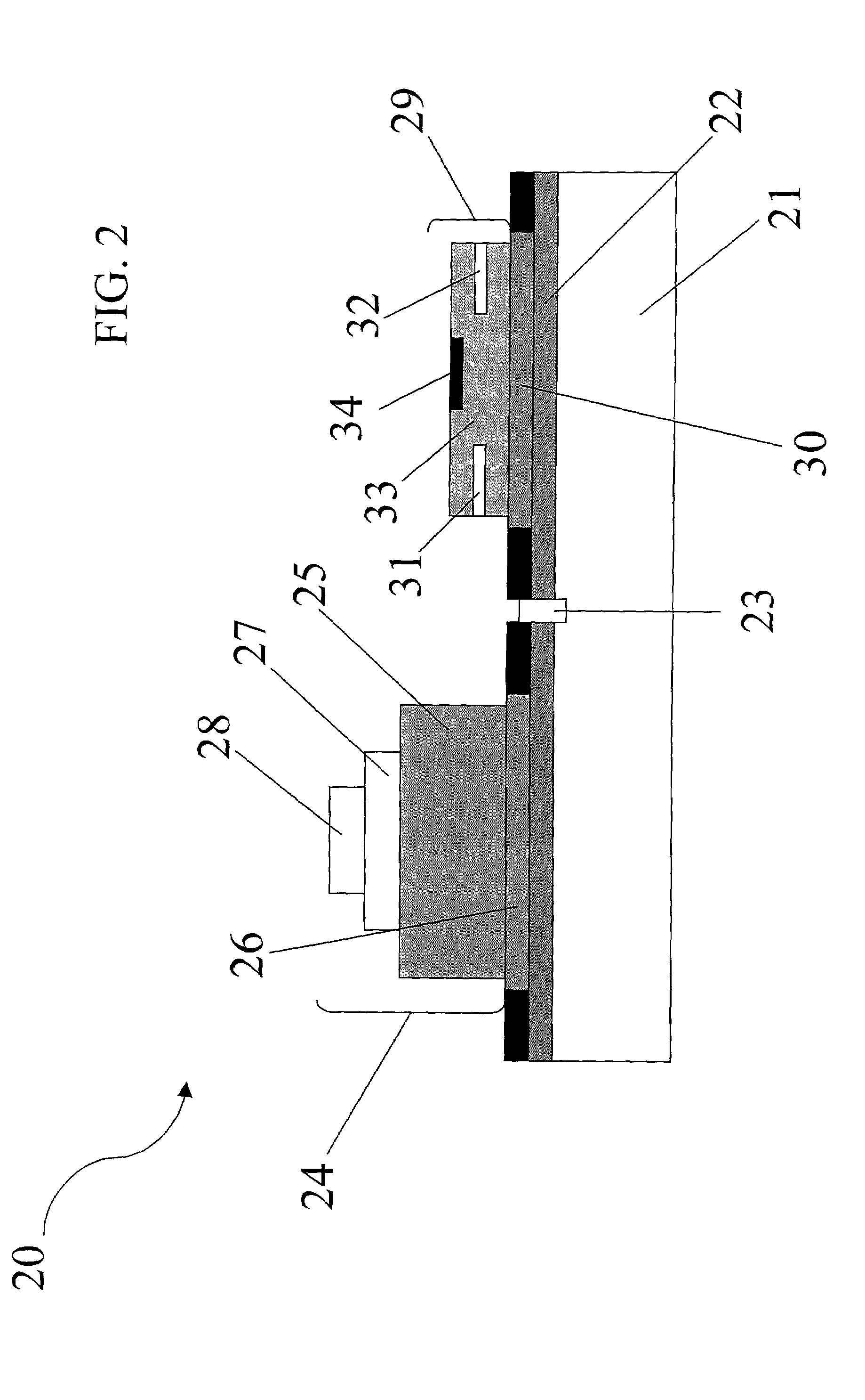
[0016]The present invention provides for a silicon carbide semi-insulating (SI) epitaxy layer used to create an entire class of power devices and integrated circuits with significant performance advantages over conventional devices. This technology is analogous to the commercially available Silicon-on-Insulator (SOI) structure, but provides advantages over the existing SOI structure, including homoepitaxy, which improves thermal conductivity and dissipation over the existing SOI structure, which is typically an insulator having significantly different thermal conductivity characteristics from the SiC based substrate upon which the structure is formed.

[0017]A requirement for electrical isolation between devices made on conducting substrates is that the epitaxial film be both thick enough and resistive enough. In general, the epitaxial film must be thicker than several diffusion lengths to ensure that carriers injected from the top by the device or from the bottom by the conducting su...


PUM


Abstract

A silicon carbide semi-insulating epitaxy layer is used to create power devices and integrated circuits having significant performance advantages over conventional devices. A silicon carbide semi-insulating layer is formed on a substrate, such as a conducting substrate, and one or more semiconducting devices are formed on the silicon carbide semi-insulating layer. The silicon carbide semi-insulating layer, which includes, for example, 4H or 6H silicon carbide, is formed using a compensating material, the compensating material being selected depending on preferred characteristics for the semi-insulating layer. The compensating material includes, for example, boron, vanadium, chromium, or germanium. Use of a silicon carbide semi-insulating layer provides insulating advantages and improved thermal performance for high power and high frequency semiconductor applications.

Description

[0001]This application claims priority from U.S. Provisional Patent Application Ser. No. 60 / 259,207 filed Jan. 3, 2001. The entirety of that provisional application is incorporated herein by reference.[0002]This invention was made with U.S. Government support under contract No. N00014-99-1-1103 awarded by the Office of Naval Research. The Government may have certain rights in this invention.BACKGROUND OF THE INVENTION[0003]1. Field of the Invention[0004]This invention relates to advanced microelectronic (semiconductor) devices and methods for fabricating the same, and in particular, to microelectronic devices employing a semi-insulating layer over a substrate.[0005]2. Background of the Technology[0006]Silicon carbide (SiC) is a rapidly maturing semiconductor technology that has excellent thermal conductivity and high breakdown strength. Wide bandgap materials, such as SiC and gallium nitride (GaN), have recently received significant attention for high frequency applications and othe...

Claims


Application Information

Patent Timeline
IPC IPC(8): H01L31/0312H01L21/04H01L21/76H01L21/8258H01L27/12H01L29/24H01L29/49H01L29/732H01L29/786H01L29/80H01L29/812
CPCH01L21/0445H01L21/7602H01L27/1203H01L29/4908H01L29/78603H01L29/78609H01L29/78684H01L29/802H01L29/812H01L29/732H01L21/8258H01L29/1608Y10S438/917Y10S438/931
Inventor CASADY, JEFFREY B.MAZZOLA, MICHAEL
Owner MISSISSIPPI STATE UNIVERSITY
Why Eureka
Try Eureka