Trench-gate semiconductor device and fabrication method thereof

a technology of a semiconductor device and a fabrication method, which is applied in the direction of semiconductor devices, electrical devices, transistors, etc., can solve the problems of difficult to maintain data-retention characteristics (generally referred to as tail characteristics) of the dram conventionally controllable with a margin, and no effective measures are found to solve the above problems, so as to improve the s parameter and the current-drive capability.

Inactive Publication Date: 2006-03-21
SONY CORP
View PDF11 Cites 25 Cited by
  • Summary
  • Abstract
  • Description
  • Claims
  • Application Information

AI Technical Summary

Benefits of technology

[0048]Further, the present inventor has considered that the deterioration in the S parameter and the current drive capability Ids can be suppressed by approximating the shape of each corner portion at the bottom of the trench to a rounded shape.
[0051]As compared with the conventional, trench gate semiconductor device wherein the corner portion between the side wall and the bottom wall of the trench is substantially right-angled, the trench gate semiconductor device according to the present invention is characterized in that the corner portion is formed by a concave surface concaved inward of the trench. Accordingly, the gate electrode and the gate insulating film have a shape corresponding to the concave surface at the bottom portion of the trench, so that field concentration occurring in the gate insulating film, especially at the corner portion in the conventional structure, can be eliminated.
[0052]As a result, the S parameter can be reduced and the current drive capability can be increased, thereby obtaining good switching characteristics with a steep slope of subthreshold current.
[0053]The switching characteristics can be improved more with an increase in the radius of curvature of the concave surface at the bottom portion of the trench.
[0054]Preferably, when the width of the trench is in the range of 40 to 250 nm, the radius of curvature r of the concave surface is set in the range of 20 nm≦r≦the width of the trench / 2. With this configuration, the radius of curvature r of the concave surface has a maximum value equal to ½ of the width of the trench. In the case that the radius of curvature r of the concave surface of each corner portion has this maximum value, the bottom of the trench becomes semicircular in cross section. In this case, the effect of suppression of the field concentration is maximized.
[0056]In the fabrication method for the trench gate semiconductor device according to the present invention, the corner portion between the side wall and the bottom wall of the trench at its bottom portion is formed by a concave surface. Accordingly, the gate electrode and the gate insulating film have a shape corresponding to the concave surface at the bottom portion of the trench, so that the field concentration occurring in the gate insulating film, especially at the corner portion in the conventional structure, can be eliminated to thereby greatly improve the S parameter and the current-drive capability.

Problems solved by technology

However, in response to a demand for annually accelerating the miniaturization of a semiconductor device, the following various problems become obvious in the Emb DRAM.
Accordingly, an electric field applied to the junction portion is becoming stronger, causing a difficulty in suppressing a leak from the junction portion to the order of ppm in a megabit-class DRAM.
As a result, the data-retention characteristics (generally referred to as Tail characteristics) of the DRAM conventionally controllable with a margin are difficult to maintain, similarly to the conventional DRAM.
In the current situation, no effective measures against the above problem are found except increasing the capacitance of a capacitor with changes in generation.
However, the aspect ratio of the word line has been increased with the recent miniaturization of the DRAM, and it has been difficult to make a sufficiently low resistance in a wiring structure of the word line for the purpose of suppressing the signal delay on the word line.
Particularly, in the Emb DRAM required to perform a high-speed operation, this signal delay on the word line is a serious problem affecting the access time to the DRAM.
However, if a salicide structure is applied to the gate electrode (word line) of a DRAM cell, offset SiO2 cannot be used to cause a hindrance to the shrinkage of the DRAM cell.
Accordingly, the use of the salicide structure for the gate electrode is difficult at present.
In activating the P+ gate electrode by heat treatment, there arises a problem of so-called “punch-through” in which the boron ions as impurities are diffused into the substrate.
As a result, there are the serious problems of variations in characteristics of the P-channel transistor, depletion of the gate electrode, and degradation in gate dielectric performance.
However, in the conventional trench gate MOSFET, as mentioned above, the channel inversion is difficult at right-angled corner portions formed by the side walls and the bottom wall of the trench 14 at its bottom portion, causing a problem that the transistor characteristics, especially the switching characteristics, do not reach an expected level.

Method used


Image

  • Trench-gate semiconductor device and fabrication method thereof
  • Trench-gate semiconductor device and fabrication method thereof
  • Trench-gate semiconductor device and fabrication method thereof

Examples


Embodiment Construction

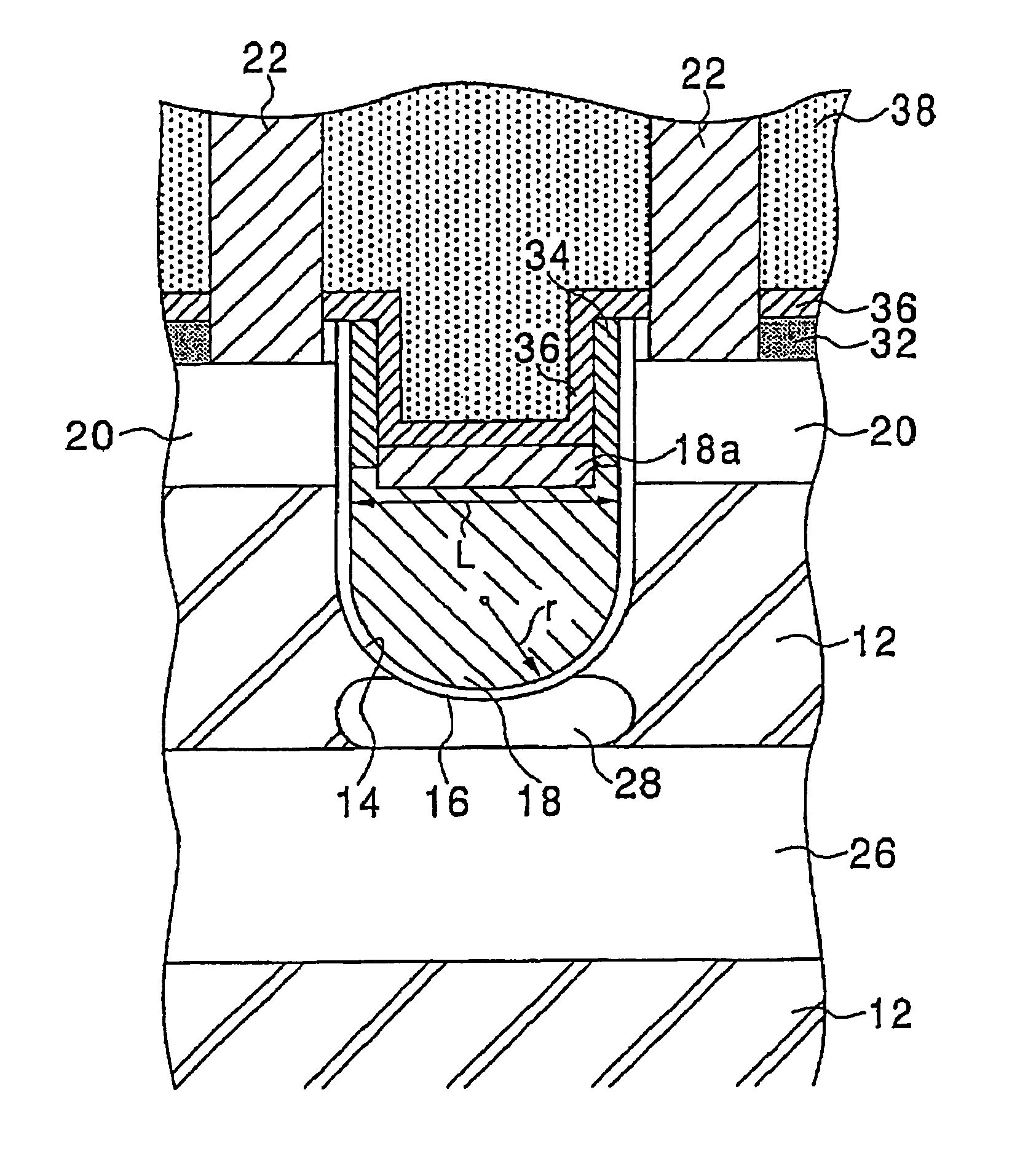
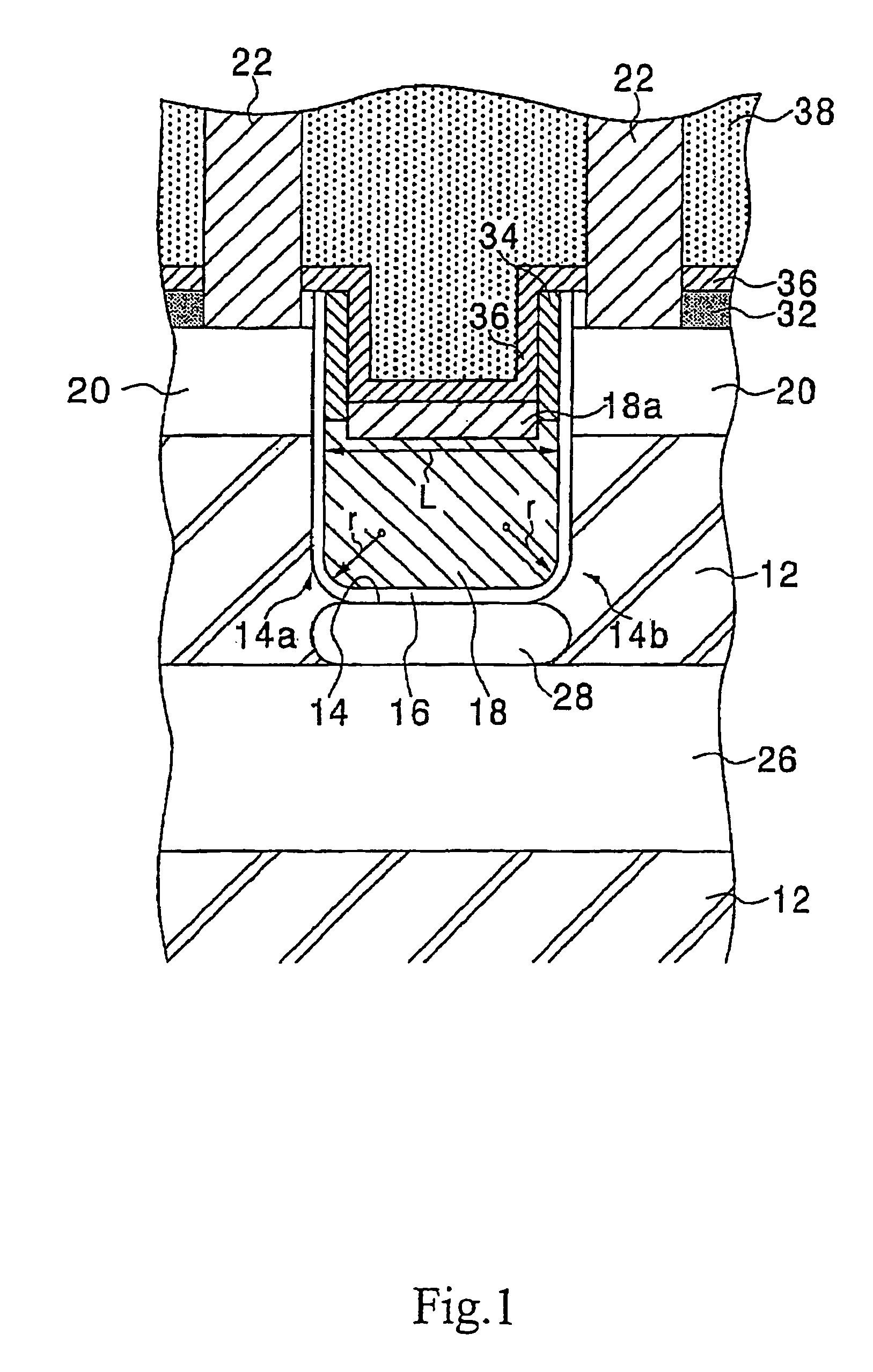
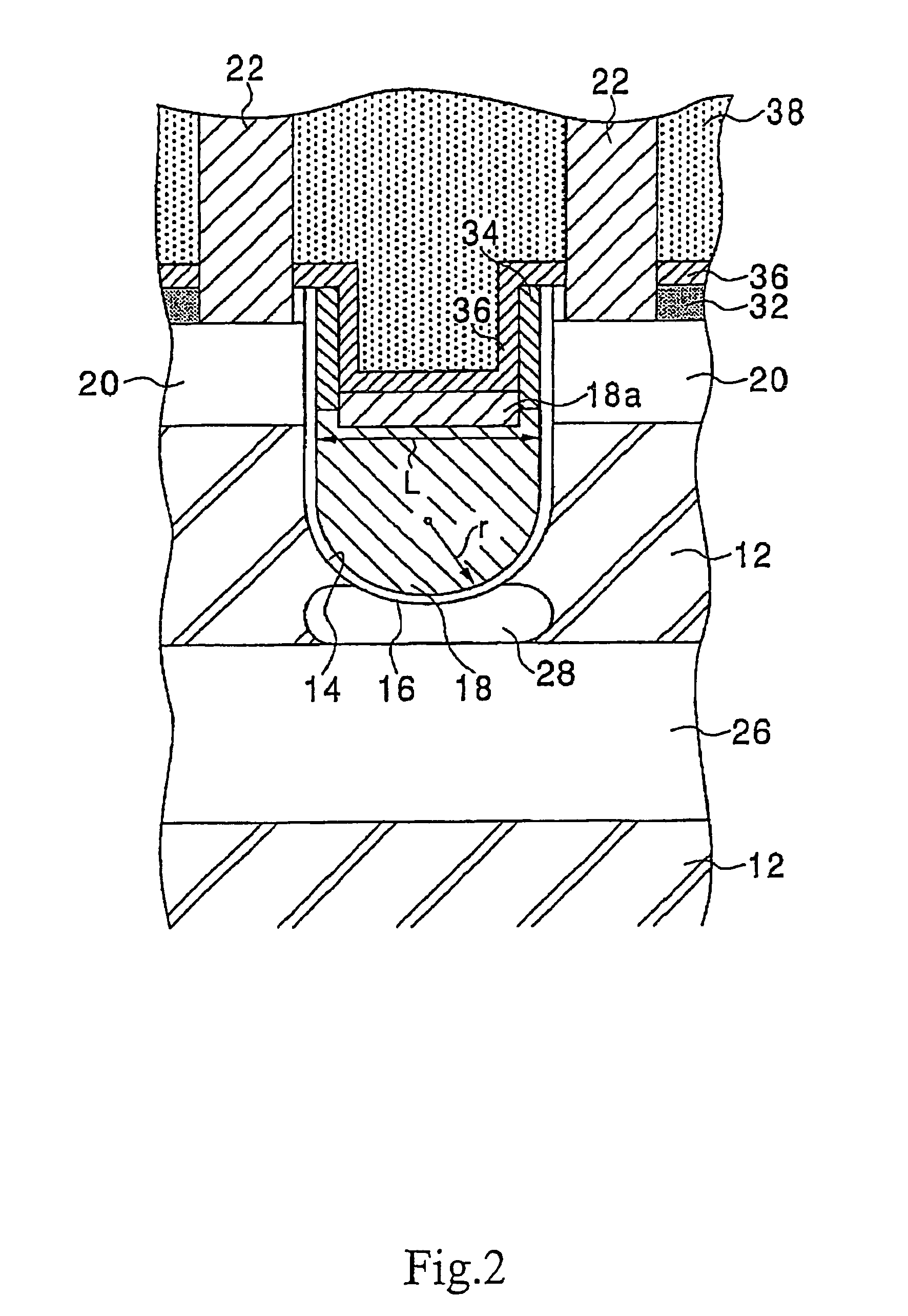
[0062]There now will be described in detail a specific preferred embodiment of the present invention with reference to the attached drawings. The configuration of a trench gate MOSFET in the preferred embodiment and a fabrication method therefor are merely illustrative for easy understanding of the present invention, and the present invention is not limited to the illustration described below.

[0063]Configuration of a Trench Gate MOSFET:

[0064]The trench gate MOSFET illustrated herein is a preferred embodiment applying the trench gate semiconductor device according to the present invention. FIG. 1 is a sectional view of an essential part of the trench gate MOSFET according to this preferred embodiment.

[0065]The trench gate MOSFET according to this preferred embodiment has the same configuration as that of the conventional trench gate MOSFET of the transistor section 10 in the TAT DRAM cell shown in FIG. 5, except for the configuration of the bottom portion of the trench 14.

[0066]As sh...


PUM


Abstract

A trench gate semiconductor device, which can improve the difficulty of channel inversion to thereby improve the switching characteristics as maintaining the effect of suppression of short-channel effects and the high dielectric voltage characteristic between the gate and the drain. The trench gate semiconductor device includes a gate electrode (18) buried in a trench (14) formed in an Si substrate (12) through a gate insulating film (16), and a source / drain diffusion layer (20) formed in a surface region of the Si substrate (12) on the opposite sides of the trench (14). In this trench gate semiconductor device, the corner portions (14a) and (14b) formed by the side walls and the bottom wall of the trench (14) are rounded so as to form concave surfaces concaved inward of the trench (14).

Description

TECHNICAL FIELD[0001]The present invention relates to a trench gate semiconductor device and a fabrication method therefor and, more particularly, to a trench gate semiconductor device which can improve transistor characteristics by the addition of a simple configuration and also to a fabrication method for such a trench gate semiconductor device.BACKGROUND ART[0002]As a semiconductor device for processing large amounts of information at high speeds, an Emb (Embedded) DRAM configured by embedding a high-capacity DRAM and a high-speed logic integrated circuit in one chip is in practical use.[0003]However, in response to a demand for annually accelerating the miniaturization of a semiconductor device, the following various problems become obvious in the Emb DRAM.[0004](1) The substrate concentration of a semiconductor substrate forming the semiconductor device is being increased, so as to maintain a high performance of a transistor against the shrinkage of a DRAM memory cell. As a res...

Claims


Application Information

Patent Timeline
Patent Type & Authority Patents(United States)
IPC IPC(8): H01L29/76H01L21/336H01L21/8242H01L27/108H01L29/78
CPCH01L27/10876H01L29/7834H01L29/66621H10B12/053H01L29/78
Inventor KAWAMURA, TAKAHIRONAKAMURA, RYOSUKE
Owner SONY CORP
Why Eureka
Try Eureka