Method for production of a semiconductor component and a semiconductor component produced by said method

a technology of semiconductor components and production methods, which is applied in the direction of fluid pressure measurement, instruments, paper/cardboard articles, etc., can solve the problems of complex production of cavities, high cost, and high cost of micromechanical bulk components, and achieve the effect of easy production and cost-effectiveness

Inactive Publication Date: 2006-05-02
ROBERT BOSCH GMBH
View PDF12 Cites 19 Cited by
  • Summary
  • Abstract
  • Description
  • Claims
  • Application Information

AI Technical Summary

Benefits of technology

[0003]The method according to the present invention may provide the advantage that a micromechanical component, e.g., a pressure sensor having piezoresistive resistors made of monocrystalline silicon, a capacitive pressure sensor, or a pressure sensor having resistors whose resistance value changes due to the deflection of a membrane of the pressure sensor when pressure is applied, may be produced easily and cost-effectively by surface micromechanics.
[0004]An aspect of the present invention is to provide a cavity in a semiconductor substrate, e.g., in a silicon substrate, using an etching medium. For this purpose, the cap layer of the substrate is etched in the region where cavities are to be produced subsequently, in such a way that openings, i.e., etched openings are made in the cap layer, e.g., pores or hollows. The etching medium or one or several subsequent etching media reach deeper regions of the substrate via the etched openings or pores, which are open to the outside. The part of the semiconductor substrate dissolved in this region by the etching medium and / or subsequent etching media may be removed via the openings, or pores of the cap layer and / or via an external access opening to this region. The cap layer may have a thickness from approximately 2 to 10 μm, e.g., 3 to 5 μm. In the case of an access opening, instead of a porous cap layer of approximately 2 to 10 μm, a porous cap layer may be produced which may have a thickness from approximately 40 to 80 μm, e.g., 50 to 60 μm. The greater thickness may allow the cap layer to be used as an etching buffer layer during the etching of the access opening and thus allowing the etching to be reliably stopped before an epitaxial layer deposited on the cap layer. In the case of a pressure sensor, the epitaxial layer deposited on the cover layer forms the actual sensor membrane.
[0007]The porosity of the cap layer may be adjustable using process technology so that it may be adequate for the removal of the silicon for producing the cavities. However, the cavities may be produced rapidly and therefore cost-effectively. According to an example embodiment of the present invention, it is provided that the etching parameters be adjusted and / or the etching medium / media for the etching of the cavity be selected so that the expansion speed of the pores and / or hollows is sufficiently high that the pores and / or hollows “overlap” with one another very rapidly. In this manner, one single largely planar starting hollow results initially in the substrate, which expands deeper as time progresses and forms the cavity.
[0012]Ethanol reduces the surface tension of an etching medium to which it is added, which allows better wetting of the silicon surface and improved penetration of the etching medium into etched pores, i.e., openings or hollows. Furthermore, the bubbles resulting during the etching procedure are smaller than those resulting without the addition of ethanol to the etching medium and the bubbles may thus escape more easily through the pores of the cap layer. Therefore, the pore size and / or the porosity of the cap layer may be kept smaller than without the addition of the alcohol.
[0019]In an example embodiment of the present invention, the support layer is produced before etching the region or the layer to be made porous by etching by providing at least the region immediately surrounding the layer to be made porous by etching of the cover area of a p-doped silicon substrate with n-doping. In this manner, “underetching” of the substrate, particularly in the region in which the porously etched layer is mechanically bonded with the silicon substrate, may be largely prevented. On the other hand, the danger exists, e.g., with a thin porous layer or starting layer, that this layer detaches from the substrate. In addition, a silicon nitride layer may be used as masking and, e.g., for protection against etching of possible underlying electronic circuits.
[0020]Alternatively or supplementarily, instead of the n-doping and / or n-doped layer, a metal layer or metal mask may be provided which also extensively prevents underetching of the substrate. The use of a metal layer and / or metal mask may be, however, only expedient, generally, if no circuits are to be provided in the substrate, since otherwise metal atoms remaining in the substrate even after the removal of the metal layer or metal mask may impair the function of the circuits.

Problems solved by technology

The production of bulk micromechanical components is relatively complicated and therefore expensive.
In conventional surface micromechanical components, the production of a cavity is complicated.
Surface micromechanical pressure sensors produced in this way also have the disadvantage that a pressure acting upon them may typically only be evaluated via a capacitive method.
Piezoresistive evaluation of the pressure acting upon them is difficult, since production of piezoresistive resistors from polycrystalline silicon is only possible through known surface micromechanical methods.
These have the disadvantage of lower long-term stability than piezoresistive resistors made of monocrystalline silicon, as well as additionally having slight piezoelectric effect.
However, the cavities may be produced rapidly and therefore cost-effectively.
On the other hand, the danger exists, e.g., with a thin porous layer or starting layer, that this layer detaches from the substrate.
The use of a metal layer and / or metal mask may be, however, only expedient, generally, if no circuits are to be provided in the substrate, since otherwise metal atoms remaining in the substrate even after the removal of the metal layer or metal mask may impair the function of the circuits.

Method used


Image

  • Method for production of a semiconductor component and a semiconductor component produced by said method
  • Method for production of a semiconductor component and a semiconductor component produced by said method
  • Method for production of a semiconductor component and a semiconductor component produced by said method

Examples


Embodiment Construction

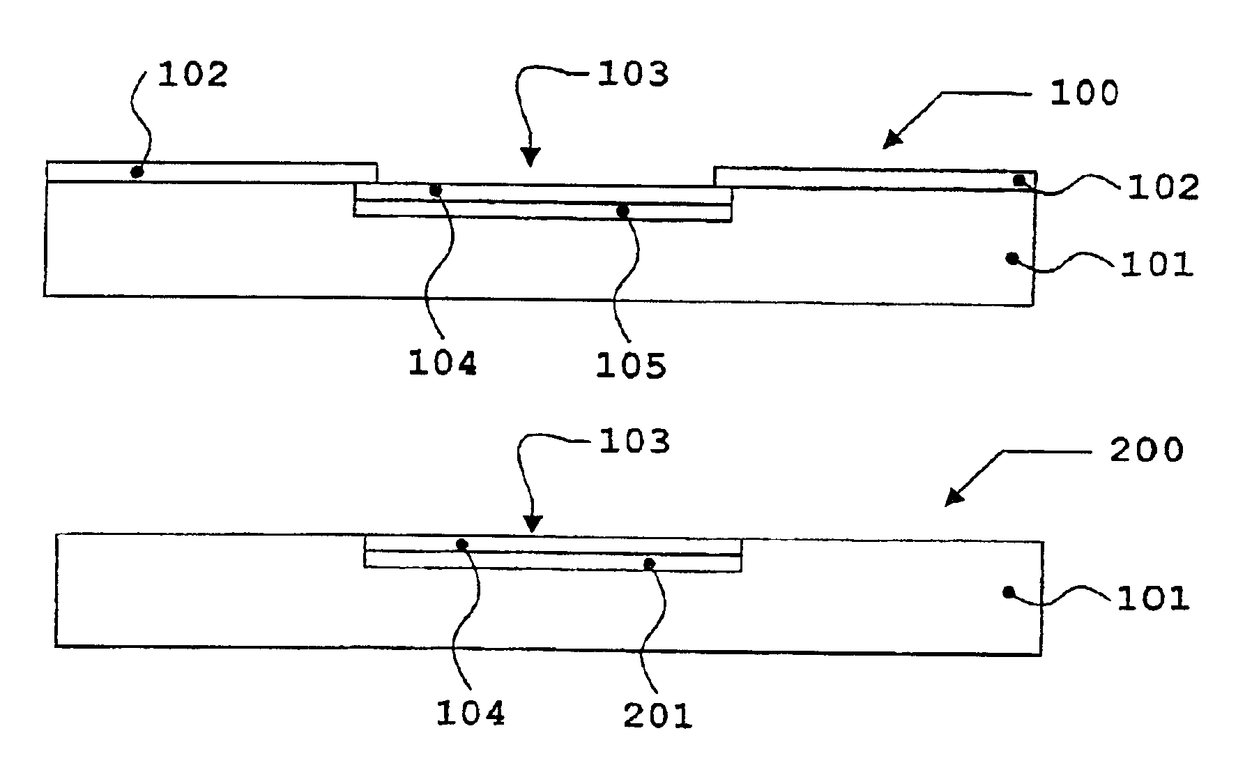
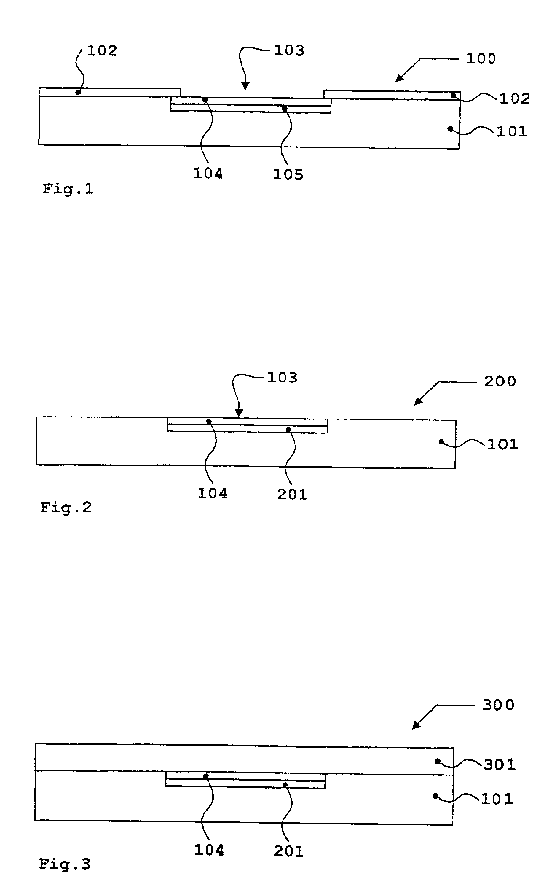
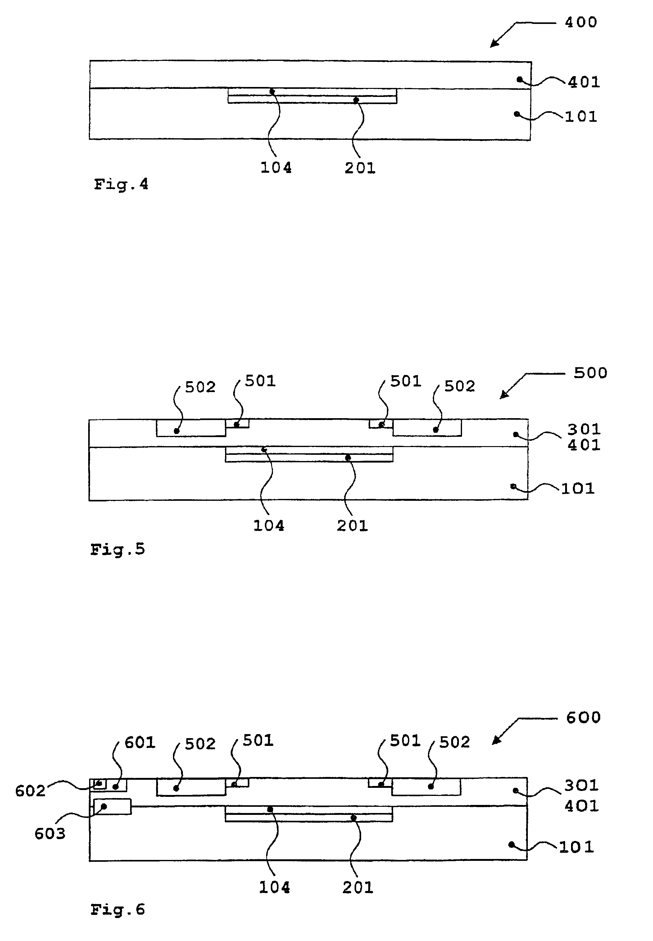
[0051]FIG. 1 is a cross-sectional view of an example embodiment of a preliminary stage 100 of absolute pressure sensor 500 illustrated in FIG. 5 To manufacture absolute pressure sensor 500 illustrated in FIG. 5, first a mask layer 102 is produced on the top of a silicon substrate 101, resulting in a region 103 not covered by mask layer 102. The mask layer may, for example, be a nitride layer, an n-doped layer (for p-doped silicon substrate), or another suitable layer which will largely not be attacked by the etching medium used subsequently.

[0052]The top of silicon substrate 101 is electrochemically etched using a suitable etching medium so that the etching medium generates small openings or pores in silicon substrate 101 directly under uncovered region 103. A silicon layer 104 having low porosity results. The etching medium reaches deep-lying regions of silicon substrate 101 through the small openings or pores of silicon layer 104 and also forms pores in the silicon located there. ...


PUM

PropertyMeasurementUnit
porosityaaaaaaaaaa
porosityaaaaaaaaaa
thicknessaaaaaaaaaa

Abstract

A method is for producing a semiconductor component, e.g., a multilayer semiconductor element, e.g., a micromechanical component, e.g., a pressure sensor, having a semiconductor substrate, e.g., made of silicon, and a semiconductor component produced according to the method. To reduce the production cost of such a semiconductor component, in a first step a first porous layer is produced in the semiconductor component, and in a second step a hollow or cavity is produced under or from the first porous layer in the semiconductor component, with the hollow or cavity capable of being provided with an external access opening.

Description

FIELD OF THE INVENTION[0001]The present invention relates to a method for producing a semiconductor component, e.g., a multilayer semiconductor component, and a semiconductor component produced according to the method.BACKGROUND INFORMATION[0002]Semiconductor components, particularly micromechanical pressure sensors, are typically produced using bulk or surface micromechanics. The production of bulk micromechanical components is relatively complicated and therefore expensive. In conventional surface micromechanical components, the production of a cavity is complicated. A typical process sequence for producing a cavity in surface micromechanics particularly includes depositing a sacrificial layer, depositing a membrane layer, which is typically made of polysilicon, producing openings in the membrane layer and / or opening a lateral etching channel, etching out the sacrificial layer, and sealing the openings, with the internal pressure of the cavity being defined upon sealing. Surface m...

Claims


Application Information

Patent Timeline
Patent Type & Authority Patents(United States)
IPC IPC(8): H01L21/302G01L9/00B81B3/00B81C1/00H01L21/306H01L29/84
CPCB81C1/00047G01L9/0045G01L9/0042H01L21/3063B81C1/00595B81B2201/0264B81B2203/0127B81B2203/0315B81C2201/0115
Inventor BENZEL, HUBERTWEBER, HERIBERTARTMANN, HANSSCHAEFER, FRANK
Owner ROBERT BOSCH GMBH
Why Eureka
Try Eureka