Single damascene integration scheme for preventing copper contamination of dielectric layer

a technology of dielectric layer and integration scheme, which is applied in the direction of semiconductor devices, semiconductor device details, electrical apparatus, etc., can solve the problems of increasing the requirements of high density and performance associated with ultra large scale integration (ulsi) semiconductor device wiring, reducing manufacturing throughput, and increasing manufacturing costs. , to achieve the effect of preventing the contamination of the dielectric layer and reducing the formation of voids

Inactive Publication Date: 2006-05-02
ADVANCED MICRO DEVICES INC
View PDF6 Cites 12 Cited by
  • Summary
  • Abstract
  • Description
  • Claims
  • Application Information

AI Technical Summary

Benefits of technology

[0027]By providing a first barrier layer to the material of the metallization layer, the material of the barrier layer can be subsequently sputtered onto the sidewalls of the via. The material deposited on the sidewalls forms a new sidewall barrier layer that prevents contamination of the dielectric layer caused by the material of the metallization layer being deposited on the sidewalls when this material is subsequently sputtered off. The sputtering process also advantageously provides the via with round corners, which reduce the formation of voids in the via.

Problems solved by technology

The escalating requirements for high density and performance associated with ultra large scale integration (ULSI) semiconductor device wiring are difficult to satisfy in terms of providing sub-micron-sized, low resistance-capacitance (RC) metallization patterns.
As integration density increases and feature size decreases, in accordance with submicron design rules, the rejection rate due to integrated circuit speed delays significantly reduces manufacturing throughput and increases manufacturing costs.
However, as the size of openings for vias / contacts and trenches is scaled down to the sub-micron range, step coverage problems result from the use of Al.
Poor step coverage causes high current density and enhanced electromigration.
Moreover, low dielectric constant polyamide materials, when employed as dielectric interlayers, create moisture / bias reliability problems when in contact with Al, and these problems have decreased the reliability of interconnections formed between various metallization layers.
For example, most W processes are complex and expensive.
Furthermore, W has a high resistivity, which decreases circuit speed.
Still a further problem is that W plugs are susceptible to void formation, and the interface with the metallization layer usually results in high contact resistance.
The use of CVD for depositing Al is expensive, and hot PVD Al deposition requires very high process temperatures incompatible with manufacturing integrated circuitry.
A problem that can be caused by the use of Cu and Cu-based alloys results from Cu having a relatively large diffusion coefficient into silicon oxide and silicon.
Once Cu has diffused into these materials, Cu can cause the dielectric strength of these materials to decrease.
Thus, if Cu from a plug or metallization layer diffuses into a silicon oxide layer, the layer can become more conductive, and this increase in conductivity can cause short circuits between adjacent conductive regions.
These short circuits can therefore result in failure of the semiconductor device.
The above-described process, however, can still result in copper contamination as a result of the use of reverse physical sputtering to clean the first metallization layer and to round the corners of the trenches and vias.
As previously stated, the diffusion of Cu into a silicon oxide dielectric layer 14 causes detrimental effects that can result in the failure of the semiconductor device.

Method used


Image

  • Single damascene integration scheme for preventing copper contamination of dielectric layer
  • Single damascene integration scheme for preventing copper contamination of dielectric layer
  • Single damascene integration scheme for preventing copper contamination of dielectric layer

Examples


Embodiment Construction

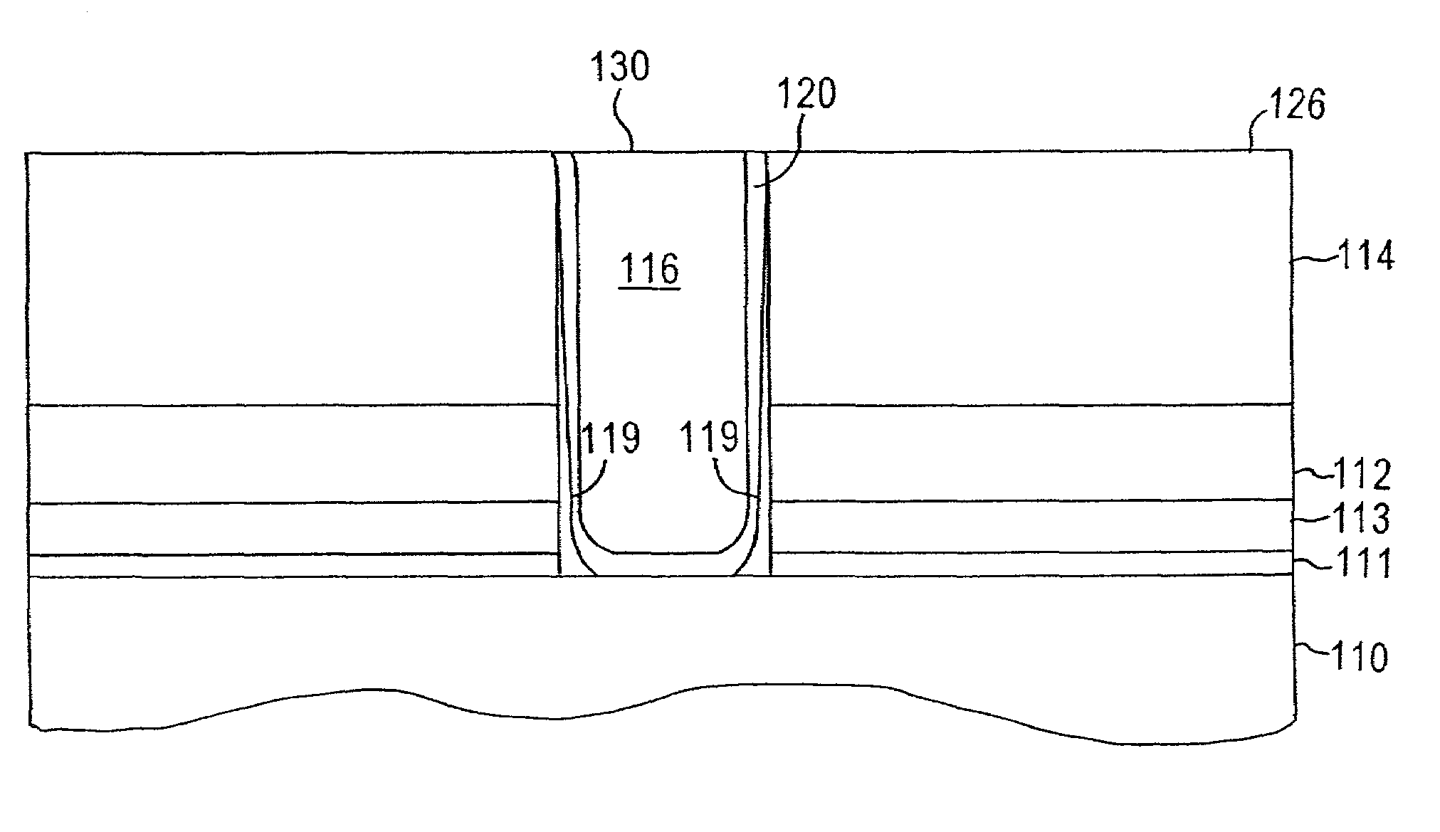
[0039]The present invention addresses and solves the problem of contamination from copper being deposited onto a silicon oxide dielectric layer as a result of reverse physical sputtering, which is used to round corners of a via and to clean contaminants on the copper metallization layer below the via. This is achieved, in part, by providing a first etch stop layer, a second etch stop layer and a barrier layer below the second etch stop layer. Advantageously, after the first etch stop layer is removed using conventional etching techniques, the second etch stop layer and the barrier layer are sputtered off during the reverse physical sputtering process. Importantly, the material of the barrier layer that is sputtered off is then deposited onto the exposed portions of the dielectric layer and creates a sidewall diffusion barrier. This is accomplished before the copper from the copper layer is sputtered off onto the dielectric layer. Thus, once the copper layer is reached during the spu...


PUM


Abstract

A semiconductor device includes a first metallization layer, a first diffusion barrier layer, a first etch stop layer, a dielectric layer and a via extending through the dielectric layer, the first etch stop layer, and the first diffusion barrier layer. The first diffusion barrier layer is disposed over the first metallization layer. The first etch stop layer is disposed over and spaced from the first diffusion barrier layer, and the dielectric layer is disposed over the first etch stop layer. The via can also have rounded corners. A second etch stop layer can also be disposed between the first diffusion barrier layer and the first etch stop layer. A sidewall diffusion barrier layer can be disposed on sidewalls of the via, and the sidewall diffusion barrier layer is formed from the same material as the first diffusion barrier layer. A method of manufacturing the semiconductor device is also disclosed.

Description

RELATED APPLICATION[0001]This application contains subject matter related to the subject matter disclosed in U.S. patent application Ser. No. 09 / 793,993, filed on Feb. 28, 2001.FIELD OF THE INVENTION[0002]The present invention relates to the manufacturing of semiconductor devices, and more particularly, to copper and copper alloy metallization in semiconductor devices.BACKGROUND OF THE INVENTION[0003]The escalating requirements for high density and performance associated with ultra large scale integration (ULSI) semiconductor device wiring are difficult to satisfy in terms of providing sub-micron-sized, low resistance-capacitance (RC) metallization patterns. This is particularly applicable when the sub-micron-features, such as vias, contact areas, lines, trenches, and other shaped openings or recesses have high aspect ratios (depth-to-width) due to miniaturization.[0004]Conventional semiconductor devices typically comprise a semiconductor substrate, usually of doped monocrystalline ...

Claims


Application Information

Patent Timeline
Patent Type & Authority Patents(United States)
IPC IPC(8): H01L23/48H01L23/52
CPCH01L21/76802H01L21/76834H01L21/76832H01L21/76814H01L21/76804
Inventor YOU, LUWANG, FEINGO, MINH VAN
Owner ADVANCED MICRO DEVICES INC
Why Eureka
Try Eureka