
Multilayer ceramic capacitor

a multi-layer ceramic and capacitor technology, applied in the field can solve the problems of frequent cause of short-circuit defective of multi-layer ceramic capacitors, inability to use costly precious metals such as platinum and palladium, and reduce permittivity largely, so as to achieve low short-circuit defective rate, avoid dc bias, and reduce the effect of cos

Active Publication Date: 2006-05-09
TDK CORPARATION
View PDF6 Cites 13 Cited by
  • Summary
  • Abstract
  • Description
  • Claims
  • Application Information

AI Technical Summary

Benefits of technology

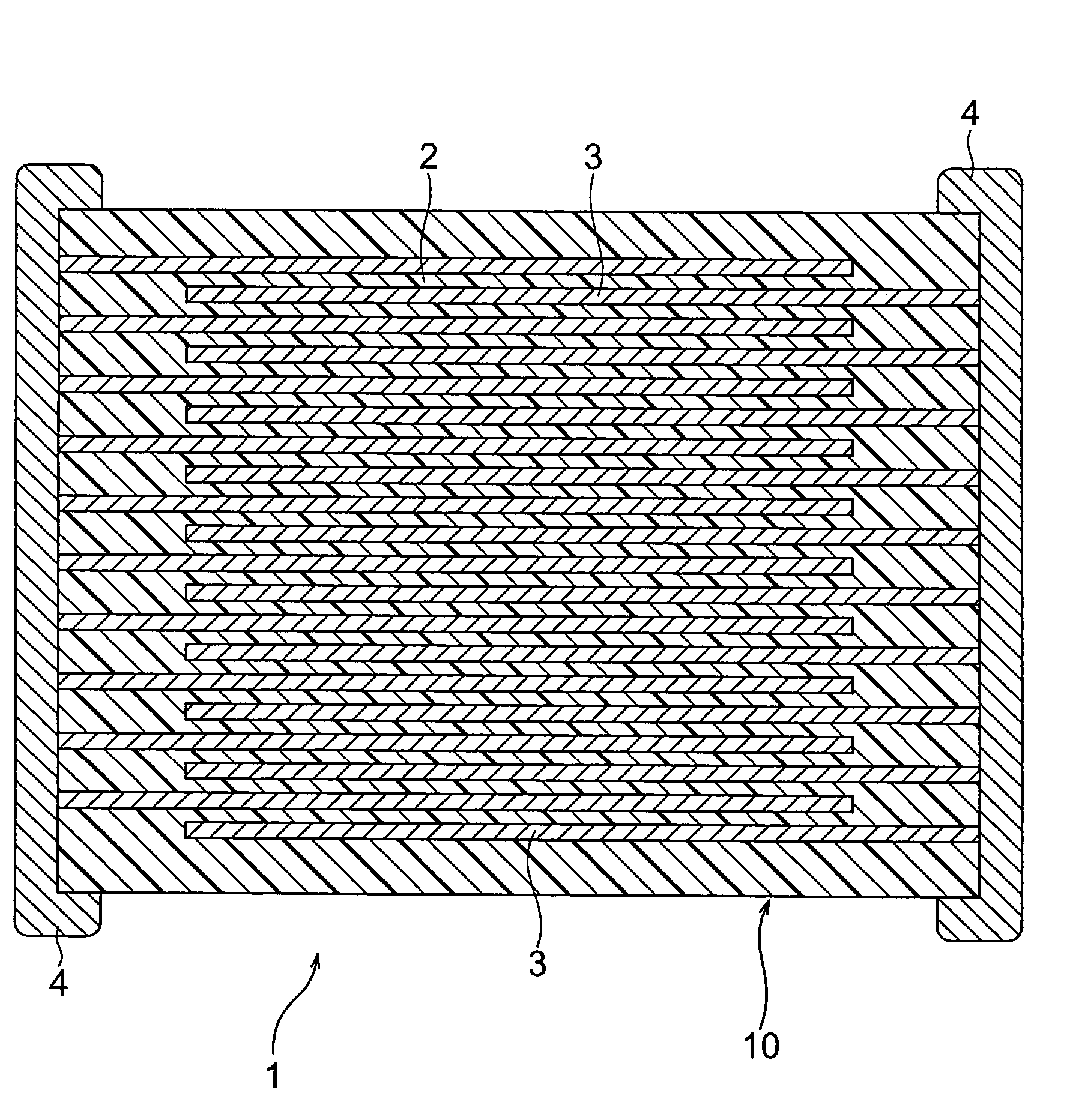
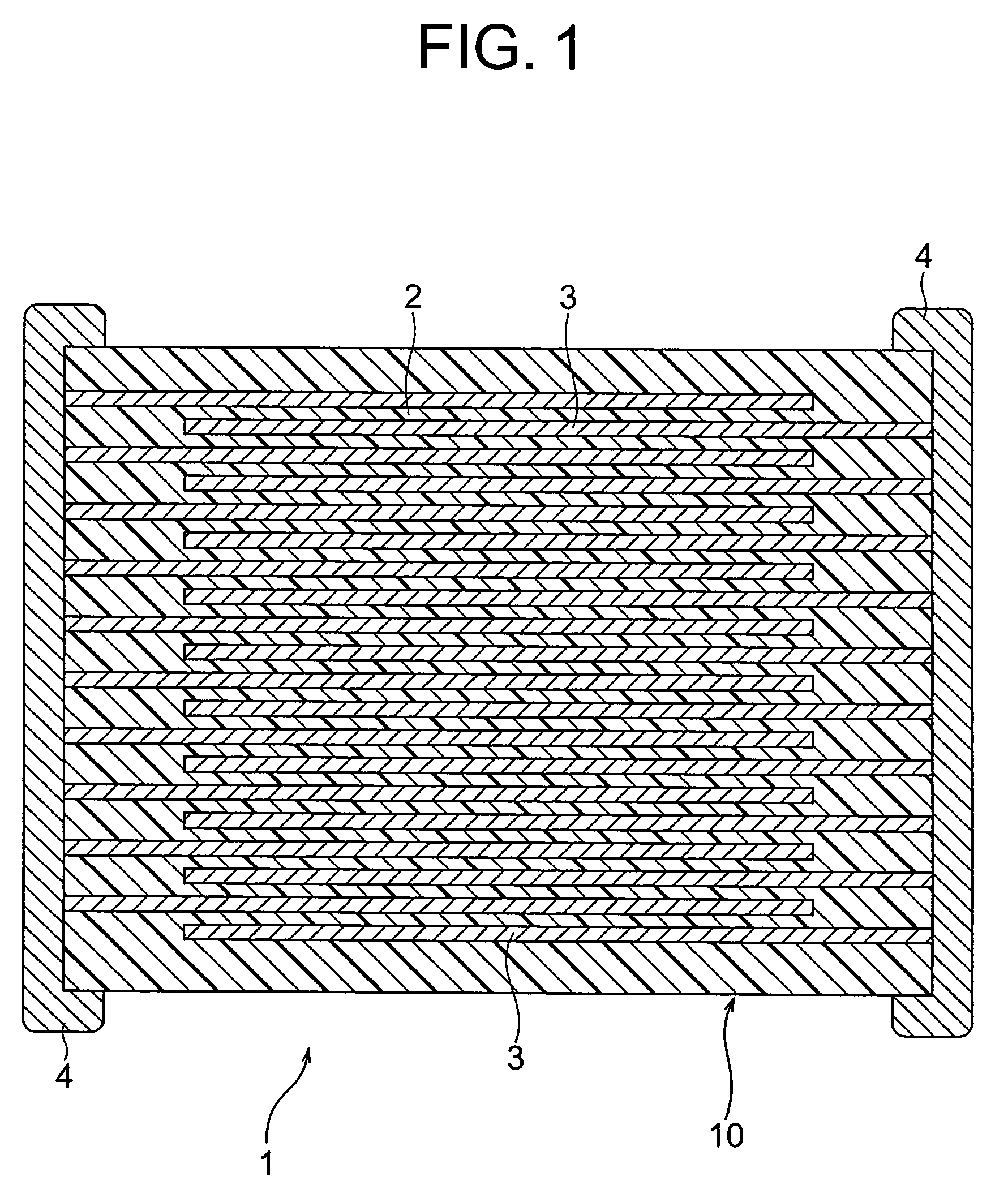
The present invention provides a multilayer ceramic capacitor with low short-circuiting defective rate, high permittivity, and preferable temperature and DC bias characteristics. By making the average particle number per one dielectric layer to 3 or more and 6 or less, the capacitor can be made thinner without compromising its performance. The dielectric layer includes a main component containing barium titanate and subcomponents such as oxides of Mg, Si, Ba, and Ca. The content of Mg oxide in the subcomponents is preferably 0.1 to 3 moles, more preferably 0.1 to 0.5 mole, and furthermore preferably 0.1 to 0.3 mole in terms of MgO with respect to 100 moles of the main component. The dielectric layer is produced by using as a material barium titanate powder having a specific surface area of 3 m2 / g or more and 10 m2 / g or less.

Problems solved by technology

Therefore, costly precious metals, such as platinum and palladium, had to be used as the material composing the internal electrode layer.
However, when a dielectric layer is made thinner, there arises a disadvantage that a short-circuiting defective of a multilayer ceramic capacitor is frequently caused.
However, when dielectric particles are made finer, the permittivity largely declines.
Accordingly, it has been considered to be difficult to suppress short-circuiting defectives and obtain a high permittivity when dielectric layers are made thinner.
Since Mg generally has a function of suppressing a peak of a permittivity at the Curies point of barium titanate, an increase of the adding quantity of Mg may lead to a problem in the temperature characteristic, particularly the temperature characteristics on the high temperature side.
However, the ceramic multilayer electronic device, particularly the ceramic multilayer electronic device disclosed in the examples disclosed in the above Japanese Unexamined Patent Publication No. 9-35985 only refers to structural defectives, such as delamination and cracks and electric characteristics thereof are unknown.
Furthermore, a thickness of a ceramic layer of the ceramic multilayer electronic device described in the examples is 5 μm, and the multilayer ceramic capacitor is hard to be compact and high in capacity with the thickness.

Method used


Image

  • Multilayer ceramic capacitor
  • Multilayer ceramic capacitor

Examples


examples

[0079]Below, the present invention will be explained further in detail based on examples, but the present invention is not limited to the examples.

[0080]As a main component, BaTiO3 materials having specific surface areas shown in Table 1 and Table 3 were prepared. Note that the specific surface area of the BaTiO3 was measured by the nitrogen absorption method (BET method). Next, the main component was added with MgO, MnO, V2O5, Y2O3, (Ba, Ca)SiO3 as subcomponents, subjected to wet mixing by a ball-mill for 16 hours and dried to obtain a dielectric material. Adding quantities of the respective subcomponents are shown in Table 1 and Table 3 by mole values with respect to 100 moles of the main components.

[0081]The obtained dielectric material was added with polyvinyl butyral and ethanol based organic solvent, mixed again with a ball-mill, and made to be a paste, so that a dielectric layer paste was obtained.

[0082]Next, 44.6 parts by weight of Ni particles, 52 parts by weight of terpine...


PUM

PropertyMeasurementUnit
thicknessaaaaaaaaaa
specific surface areaaaaaaaaaaa
particle diameteraaaaaaaaaa

Abstract

A multilayer ceramic capacitor having internal electrode layers and dielectric layers, wherein a thickness of said dielectric layer is 2.0 μm or less, and an average particle number per one dielectric layer obtained by dividing the thickness of said dielectric layer by an average particle diameter of dielectric particles composing said dielectric layer is 3 or more and 6 or less.

Description

BACKGROUND OF THE INVENTION[0001]1. Field of the Invention[0002]The present invention relates to a multilayer ceramic capacitor, and particularly relates to a multilayer ceramic capacitor ready for a small size and large capacity.[0003]2. Description of the Related Art[0004]A multilayer ceramic capacitor as an example of electronic devices is produced, for example, by printing a predetermined pattern of internal electrodes on a ceramic green sheet made by a predetermined dielectric ceramic composition, stacking a plurality of the results, then unifying the same, and cofiring a thus obtained green chip. It is necessary that a material which does not react with a ceramic dielectric has to be selected for the internal electrode layer of the multilayer ceramic capacitor so as to be unified with the ceramic dielectric by firing. Therefore, costly precious metals, such as platinum and palladium, had to be used as the material composing the internal electrode layer.[0005]However, in recent...

Claims


Application Information

Patent Timeline
Patent Type & Authority Patents(United States)
IPC IPC(8): H01G4/06C01G23/00C04B35/468C04B35/638C04B35/64H01G4/12H01G4/30
CPCB32B18/00H01G4/30C04B35/4682C04B35/63C04B35/6303C04B35/638C04B35/64H01G4/1209H01G4/1227C04B2235/3206C04B2235/3215C04B2235/3225C04B2235/3236C04B2235/3239C04B2235/3267C04B2235/3418C04B2235/3436C04B2235/3454C04B2235/5409C04B2235/5445C04B2235/652C04B2235/6582C04B2235/6584C04B2235/662C04B2237/346C04B2237/405C04B2237/704B32B2311/22H01G4/12
Inventor UMEDA, YUJISATO, AKIRA
Owner TDK CORPARATION
Learn More