Production method for semiconductor crystal and semiconductor luminous element
Inactive Publication Date: 2006-05-30
TOYODA GOSEI CO LTD
View PDF102 Cites 59 Cited by
Summary
Abstract
Description
Claims
Application Information
AI Technical Summary
This helps you quickly interpret patents by identifying the three key elements:
Problems solved by technology
Method used
Benefits of technology
Benefits of technology
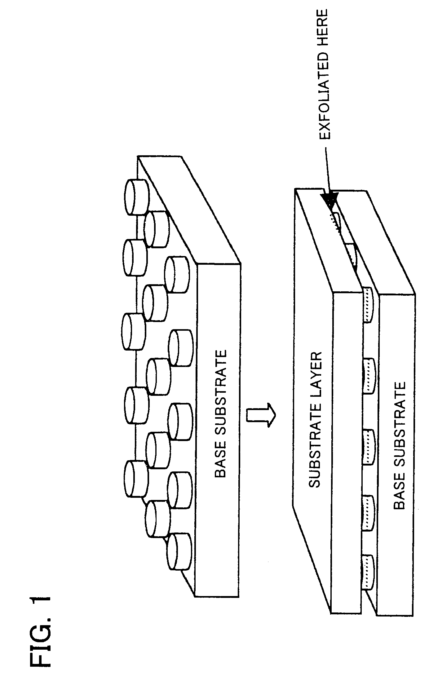
[0015]Although the base substrate except for the objective grown layer is removed so as to obtain a free-standing substrate (crystal), the substrate cannot have larger area because of dislocations and cracks described above. When the objective single crystal is grown in a certain thickness, cracks are generated in the objective single crystal even during the growth process. That easily causes problems such that small pieces are partially peeled off.
[0221]Alternatively, in the separation process, in order to decrease a temperature of the base substrate and the substrate crystal A, they may be preferably left in a reaction chamber of a growth apparatus and cooled to approximately ambient temperature at a cooling rate of about −100° C. / min to −0.5° C. / min under condition that ammonia (NH3) gas is flown at an approximately constant flowing rate. As a result, the separation process may be carried out by keeping crystallinity of the semiconductor crystal A stable and excellent.
Problems solved by technology
When a number of dislocations and cracks are generated in the grown layer (nitride semiconductor layer), a number of lattice defects, dislocations, deformation, cracks, etc., are generated in a device fabricated on the semiconductor layer, thereby deteriorating device characteristics.
Dislocations and cracks are occurred because of stress which is generated owing to difference of thermal expansion coefficients and difference of lattice constants between different kinds of materials.
So when such a crystal growth substrate is used for fabricating each kind of semiconductor devices, device characteristics of the device is deteriorated.
As a result, it is not easy to obtain a single crystalline GaN substrate by applying a crystal growing process in a high temperature.
Method used
Image
Click on the blue label to locate the original text in one second.
Reading with bidirectional positioning of images and text.
Examples
first embodiment
[1] Projection part forming process
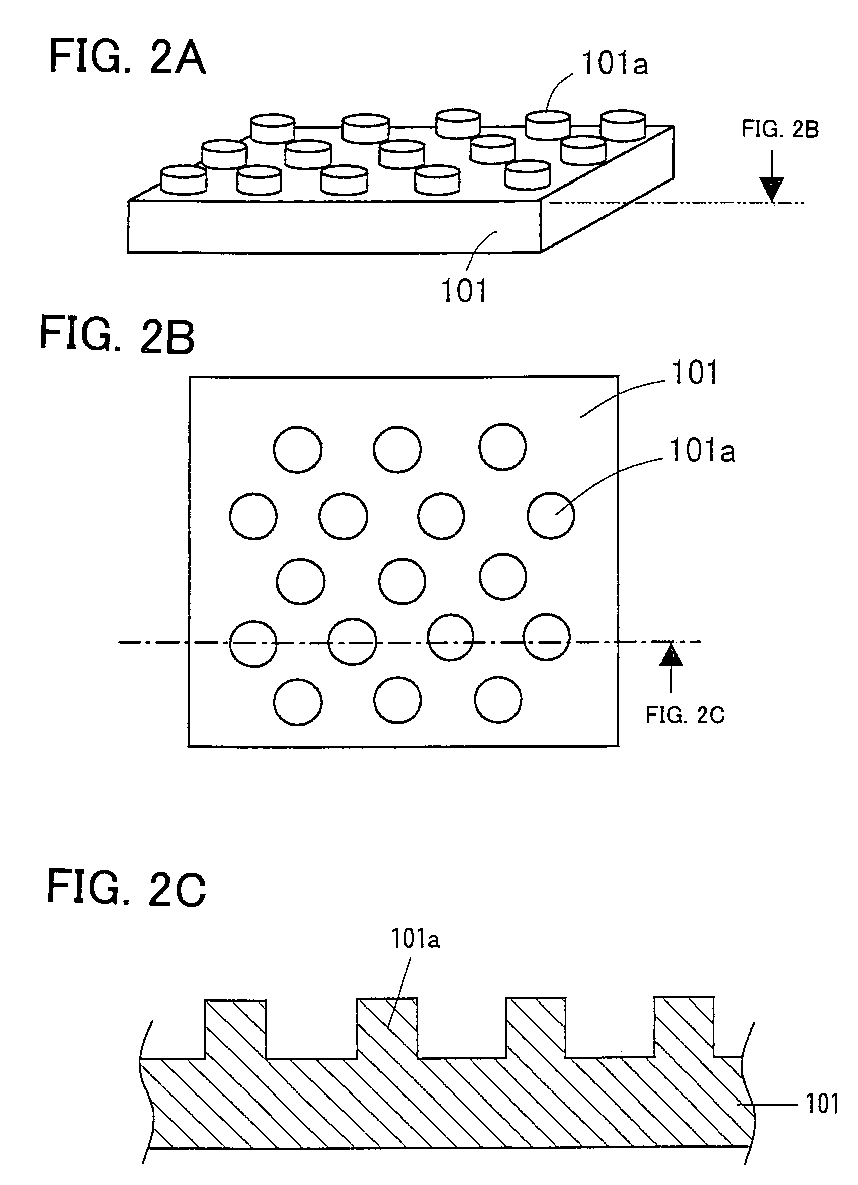
[0236]As shown in FIGS. 2A–2C, projection parts 101a each having diameter of approximately 1 μm and height of approximately 1 μm are formed in an approximately columnar shape on a Si (111) plane of a base substrate 101 made of Si single crystal at an interval of about 2 μm through dry-etching using photolithography. Each of the projection part 101a is arranged so that the center of the columnar bottom is placed at each lattice point of a two-dimensional triangle lattice based on an approximately equilateral triangle whose edge is about 2 μm. Here a thickness of the base substrate 101 is about 200 μm.
[0237]In the crystal growing process, the upper surface of the projection part 101a (at an initial state) is connected with each other to be a series of an approximately plane growth surface of a crystal as shown in FIGS. 4A–4C through metal-organic vapor phase epitaxy (hereinafter called “MOVPE”). After that the substrate lay...
second embodiment
[0264]In the following Example, a method for producing a semiconductor crystal (crystal growth substrate) according to a second embodiment of the present invention will be described.
[1] Reaction Prevention process
[0265]A reaction prevention process is a process for depositing a reaction prevention layer on a base substrate (Si substrate).
[0266]In this process, first, about 1.5 μm in thickness of a reaction prevention layer made of siliconcarbide (SiC) is formed on the Si (111) substrate through chemical vapor deposition (CVD). In order to prevent a wafer from curving, a SiC film may be formed on both the surface and the back surface of the substrate. Alternatively, the siliconcarbide (SiC) may be formed through metal-organic vapor phase growth (MOCVD).
[2] Projection part forming process
[0267]Projection parts B1 each having diameter of approximately 1 μm and a height of approximately 1 μm are formed in an approximately columnar shape on the reaction prevention layer at an interval ...
third embodiment
1. Seed depositing process
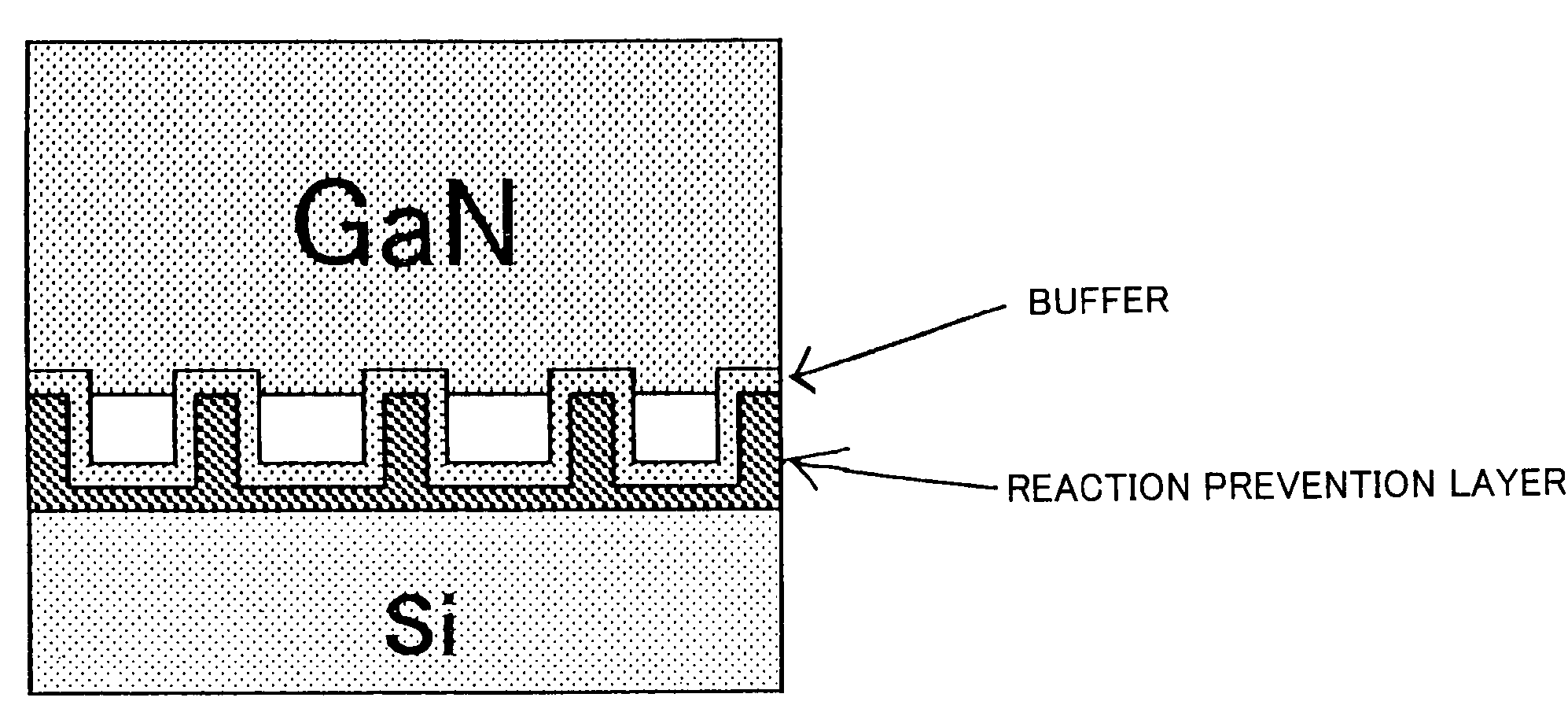
[0285]In this embodiment, a seed layer (group III nitride compound semiconductor) comprising a first seed layer (AlN buffer layer 102) and a second seed layer (GaN layer 103) was formed through metal-organic vapor phase epitaxy (“MOVPE” hereinafter). In this process, the following gasses were employed: ammonia (NH3), carrier gas (H2 or N2), trimethylgallium (Ga(CH3)3, hereinafter called “TMG”), and trimethylaluminum (Al(CH3)3, hereinafter called “TMA”).
[0286]FIGS. 9A–9C are schematic sectional views of a semiconductor crystal illustrating producing process of the semiconductor crystal of the present invention.
[0287]First, a sapphire substrate 101 (base substrate) which is 1 inch square and has a thickness about 250 μm was cleaned by organic washing solvent and heat treatment (baking). Then about 200 nm in thickness of AlN buffer layer 102 (first seed layer) was formed by crystal growth on a main surface ‘a’ of the single crystalline base substrate 101, whic...
PUM
Abstract
When a substrate layer (desired semiconductorcrystal) made of a group III nitride compound is grown on a base substrate comprising a lot of projection parts, a cavity in which a semiconductorcrystal is not deposited may be formed between each projection part although it depends on conditions such as the size of each projection part, arranging interval between each projection part and crystal growth. So when the thickness of the substrate layer is sufficiently larger compared with the height of the projection part, inner stress or outer stress become easier to act intensively to the projection part. As a result, such stress especially functions as shearing stress toward the projection part. When the shearing stress becomes larger, the projection part is ruptured. So utilizing the shearing stress enables to separate the base substrate and the substrate layer easily. The larger the cavities are formed, the more stress tends to concentrate to the projection parts, to thereby enable to separate the base substrate and the substrate layer more securely.
Description
TECHNICAL FIELD[0001]The present invention relates to a method for producing semiconductor crystal comprising a step of forming a substrate layer comprising group III nitridecompound semiconductor on a base substrate using lateral crystal growth effect to thereby obtain a substrate for a crystal growth.[0002]And the present invention relates to a method for producing a semiconductor substrate by growing a crystal of group III nitridecompound semiconductor on a base substrate consisting of silicon (Si). The present invention also relates to a group III nitride compound semiconductor device formed on such a semiconductor substrate obtained by above method.[0003]Further, the present invention relates to a method for growing a semiconductor crystal made of group III nitride compound semiconductor on a base substrate, to thereby obtain a semiconductor crystal which has excellent quality and is independent from the base substrate.[0004]And the present invention can be applied to a produ...
Claims
Application Information
Patent Timeline
Application Date:The date an application was filed.
Publication Date:The date a patent or application was officially published.
First Publication Date:The earliest publication date of a patent with the same application number.
Issue Date:Publication date of the patent grant document.
PCT Entry Date:The Entry date of PCT National Phase.
Estimated Expiry Date:The statutory expiry date of a patent right according to the Patent Law, and it is the longest term of protection that the patent right can achieve without the termination of the patent right due to other reasons(Term extension factor has been taken into account ).
Invalid Date:Actual expiry date is based on effective date or publication date of legal transaction data of invalid patent.

