

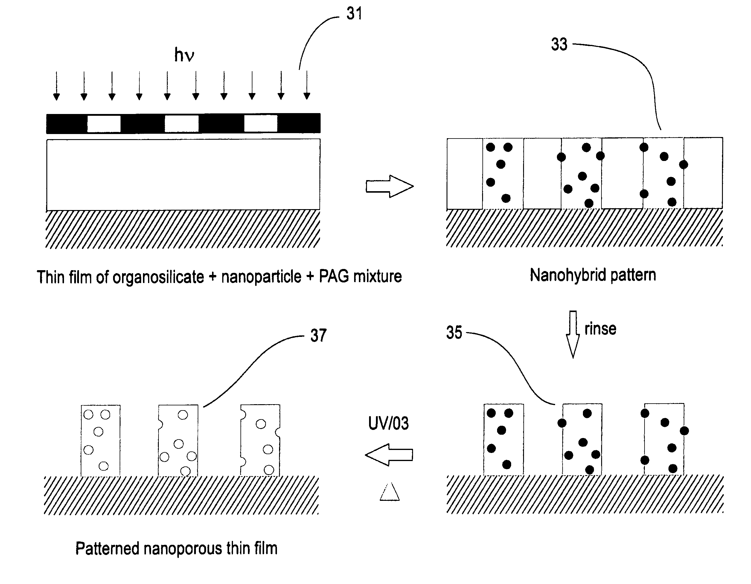
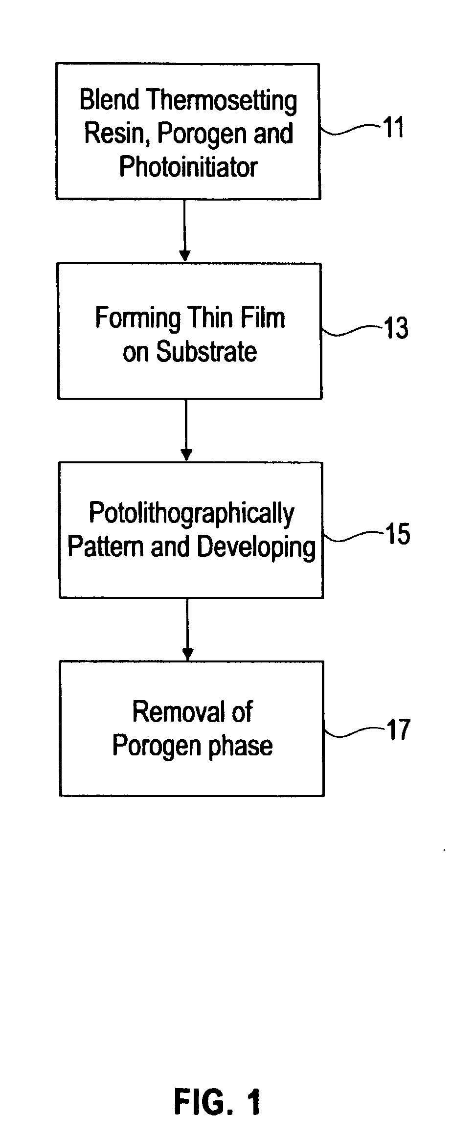
Direct photo-patterning of nanoporous organosilicates, and method of use
a nanoporous organosilicate and nanoporous material technology, applied in the direction of organic compounds/hydrides/coordination complex catalysts, physical/chemical process catalysts, instruments, etc., can solve the problems of increasing the delay and signal degradation of the back-end-of-line (beol) wiring of semiconductor chips, and the limited porous films in these studies, so as to achieve simple oxidation methods
- Summary
- Abstract
- Description
- Claims
- Application Information
AI Technical Summary
Benefits of technology
Problems solved by technology
Method used
Image

Examples
example 1
[0053]FIG. 9 shows the index of refraction RI of porous methyl silsequioxanes made from three different porogens, confirming that the structures are porous. The porogens for nucleation and growth (linear alkylene oxide) and templating (amphiphilic core shell particles) processes generate almost the same degree of porosity in organosilicate films. The refractive index determined at 632.8 nm decreases from 1.37 to 1.14 as the porogen load is increased from 0% to 60%; hence, the dielectric constant must also decrease with increased porogen loading.
example 2
[0054]A mixture was prepared by dissolving methyl silsesquioxane (MSSQ), amphiphilic polystyrene core / polyethylene oxide methacrylate shell sacrificial organic porogen nanoparticles, and bis-t-butyl phenyl iodonium triflate photoacid generator in propylene glycol methyl ether solvent. The mixture, which was 30 wt. % porogen and 10 wt. % photoacid generator, was spin coated onto Si substrates. Typical film thicknesses were about 1 μm. The films were prebaked for 1 min at 100° C., and then exposed to UV radiation (254 nm) through a photomask. The patterns were developed by rinsing with propylene glycol methyl ether. To generate a porous structure, the patterned film was annealed at 450° C. for two hours. The refractive index was determined at 632.8 nanometers.
[0055]FIG. 10 shows optical microscope images of the patterned surfaces. Well-defined features (patterns) with sizes ranging from 50 μm to 500 μm are shown in the images of FIG. 10. As shown in FIG. 11, Field Emission Scanning El...
example 3
[0056]Further tests were carried out to determine the spatial density of patterns obtained using the method described in Example 2. FIG. 12, shows 1, 2, 4, and 8 micrometer feature sizes obtained using the method of the invention.
PUM
| Property | Measurement | Unit |
|---|---|---|
| size | aaaaa | aaaaa |
| dielectric constant | aaaaa | aaaaa |
| refractive index | aaaaa | aaaaa |
Abstract
Description
Claims
Application Information