Light-emitting apparatus, phosphor, and method of producing it

a technology of light-emitting apparatus and phosphor, which is applied in the direction of discharge tube/lamp details, semiconductor lasers, discharge tubes luminescnet screens, etc., can solve the problems of shortening the lifetime of excitation light sources, increasing power consumption, and difficulty in realizing light-emitting apparatuses. achieve the effect of high resolution and enhance the quantum efficiency of phosphor

Active Publication Date: 2006-06-06
SHARP KK
View PDF5 Cites 44 Cited by
  • Summary
  • Abstract
  • Description
  • Claims
  • Application Information

AI Technical Summary

Benefits of technology

[0036]In a light-emitting apparatus structured as described above according to the present invention, a phosphor is formed of crystals having a particle diameter equal to or smaller than twice the exciton Bohr radius. Thus, by exciting this phosphor with light ...

Problems solved by technology

Inconveniently, this increases power consumption and shortens the lifetime of the excitation light source.
For this reason, it has to date been difficult to realize a light-e...

Method used


Image

  • Light-emitting apparatus, phosphor, and method of producing it
  • Light-emitting apparatus, phosphor, and method of producing it
  • Light-emitting apparatus, phosphor, and method of producing it

Examples


example 1

[0063]A light-emitting apparatus structured as shown in FIG. 3A was fabricated.

Primary Light Source

[0064]In this example, a stripe laser structured as shown in FIG. 8, i.e., one having a ridge structure, was fabricated as the primary light source. In the following description, the values given in cm−3 are carrier densities.

Laser

[0065]As shown in FIG. 8, on top of a GaN substrate 80, an n-GaN contact layer 81 (3 μm thick, 1×1018 cm−3), an n-Al0.1Ga0.9N clad layer 82 (1 μm thick, 1×1018 cm−), an n-GaN guide layer 83 (0.1 μm thick, 1×1018 cm−3), an In0.15Ga0.85N / In0.05Ga0.95N 3MQW active layer 84, a p-Al0.15Ga0.85N evaporation prevention layer 85 (0.02 μm thick, 1×1018 cm−3), a p-GaN guide layer 86 (0.1 μm thick, 1×1018 cm−3), a p-Al0.1Ga0.9N clad layer 87 (0.6 μm thick, 1×1018 cm−3), and a p-GaN contact layer 88 (0.1 μm thick, 1×1018 cm−3) were laid on one another.

[0066]Next, by RIE, this multilayer structure was partially etched from the top surface thereof so that the p-AlGaN clad l...

example 2

[0070]A light-emitting apparatus structured as shown in FIG. 3B was fabricated.

Primary Light Source

[0071]As the primary light source, the same laser as used in Example 1 was used.

Phosphor

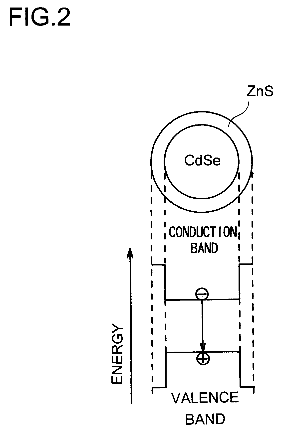
[0072]InN nano-crystals having volumes of 3.375 nm3 to 64 nm3 (1.5 nm to 4 nm along each side) were grown by laser ablation, and then, on top of the InN, GaN was grown by laser ablation in a similar manner to produce InN / GaN nano-crystals having a quantum well structure as shown in FIG. 2. Then, acrylic resin having these nano-crystals dispersed therein was formed into a cylindrical shape. The reason that the volume varied from 3.375 nm3 to 64 nm3 (1.5 nm to 4 nm along each side) was that the volume that produced the same phosphorescence wavelength varied according to the conditions of growth.

Evaluation

[0073]When the laser of the above light-emitting apparatus was energized to cause laser oscillation, phosphorescence of a wavelength 520 nm was obtained with energy conversion efficiency of 120 [lm / W]...

example 3

[0075]A light-emitting apparatus structured as shown in FIG. 4 was fabricated.

Primary Light Source

[0076]In this example, an LED structured as shown in FIG. 10 was fabricated. In the following description, the values given in cm−3 are carrier densities.

Laser

[0077]As shown in FIG. 10, on top of a sapphire substrate 90, a buffer layer (not shown) was grown, and then an n-GaN contact layer 91 (3 μm thick, 1×1018 cm−3), an In0.12Ga0.87N / GaN 5MQW active layer 92, a p-Al0.15Ga0.85N evaporation prevention layer 93 (0.02 μm thick, 1×1018 cm−3), a p-GaN contact layer 94 (0.2 μm thick, 1×1018 cm−3), an laid on one another. Next, by RIE, this multilayer structure was partially etched from the top surface thereof so that the n-GaN contact layer 91 was exposed except for a portion thereof. Then, on top, an n-type electrode 95 (Ti / Al) was formed. Moreover, on top of the p-GaN contact layer 94, a p-type transparent electrode 96 (Pd; 0.008 nm) was formed, and on top of a portion thereof, a p-type el...


PUM

PropertyMeasurementUnit
Fractionaaaaaaaaaa
Fractionaaaaaaaaaa
Volumeaaaaaaaaaa

Abstract

A light-emitting apparatus composed of a light source that emits primary light and a phosphor that absorbs the primary light and emits secondary light offers high brightness, low power consumption, and a long lifetime while minimizing adverse effects on the environment. The phosphor is formed of a III–V group semiconductor in the form of fine-particle crystals each having a volume of 2 800 nm3 or less. The light emitted from the fine-particle crystals depends on their volume, and therefore giving the fine-particle crystals a predetermined volume distribution makes it possible to adjust the wavelength range of the secondary light.

Description

BACKGROUND OF THE INVENTION[0001]1. Field of the Invention[0002]The present invention relates to a light-emitting apparatus, and more particularly to a light-emitting apparatus that irradiates a phosphor with primary light emitted from a primary light source and that thereby produces secondary light having longer wavelengths than the primary light.[0003]2. Description of the Prior Art[0004]GaN-based semiconductors are direct-transition semiconductors with band gaps ranging from 0.9 eV or 1.8 eV to 6.2 eV, and thus they make it possible to realize light-emitting devices that emit light in a wide band ranging from visible to ultraviolet regions. For this reason, in recent years, GaN-based semiconductors have been receiving much attention and have been actively developed. The reason that the lower limit of the band gap is given as 0.9 eV or 1.8 eV above is that the band gap of InN has not yet been definitely determined between two theories that support 0.9 eV and 1.8 eV respectively.[0...

Claims


Application Information

Patent Timeline
IPC IPC(8): H01S3/08B82B1/00B82B3/00B82Y20/00B82Y30/00B82Y40/00C09K11/08C09K11/62C09K11/64H01S5/022H01S5/323H01S5/343
CPCB82Y20/00C09K11/0883C09K11/62H01L33/502H01S5/34333H01S5/005H01S5/02284H01S5/02296Y10S977/783Y10S977/815Y10S977/816H01S5/02251H01S5/02257H01S5/0078H01S5/0087H01S5/0225H01S5/32341H01S5/22
Inventor ISHIDA, MASAYAMORIOKA, TATSUYAHANAOKA, DAISUKETANEYA, MOTOTAKAFUJITA, SHIGEOKAWAKAMI, YOICHIHARADA, MASAFUMISASAKI, TAKATOMOMORI, YUSUKE
Owner SHARP KK
Why Eureka
Try Eureka