Integrated optical circuits

a technology of integrated optical circuits and optical circuits, applied in the direction of active medium materials, instruments, semiconductor lasers, etc., can solve the problems of large volume, large complexity, and obstacles to the total realization of an all-optical network, and achieve the effect of large-volume ready-to-fabrication

Inactive Publication Date: 2006-06-06
GULA CONSULTING LLC +1
View PDF142 Cites 67 Cited by
  • Summary
  • Abstract
  • Description
  • Claims
  • Application Information

AI Technical Summary

Benefits of technology

[0017]A class of sol-gel based optical components, devices and subsystems are therefore provided that benefit from fabrication techniques that allow complex optical circuitry to be integrated in an all-optical environment. By leveraging emerging MEMS ...

Problems solved by technology

However, barriers still exist that prevent the total realization of an all-optical network.
One key problem for both telecommunications and data communications in an all-optical environment is in the area of integration, i.e. being able to integrate and connect a myriad of optical devices in a confined space.
In this regard, the increasing sophistication of the network leads to greater complexity.
However, the increasing density of these cable connections is creating problems in cable management, resulting in incorrect or unidentified connections.
Other trouble spots include reliability, cost, and space consumption.
For this reason their implementation has been limited to relatively short distances.
Therefore, the integration and packaging of such backplanes have been and still remain a major challenge.
Traditional work in the area of sol-gel based interconnects/waveguides have required high temperature processing and, therefore has resulted in devices having high optical loss.
As such, the underlying substrate is limited to materials that can withstand this high temperature processing, such as glass.
Additionally, rare earth ion (erbium, ytterbium, etc.) doping of sol-gel to create active regions within the waveguides has been limited to traditional high tem...

Method used


Image

  • Integrated optical circuits
  • Integrated optical circuits
  • Integrated optical circuits

Examples


Embodiment Construction

[0050]The present invention now will be described more fully hereinafter with reference to the accompanying drawings, in which preferred embodiments of the invention are shown. This invention may, however, be embodied in many different forms and should not be construed as limited to the embodiments set forth herein; rather, these embodiments are provided so that this disclosure will be thorough and complete, and will fully convey the scope of the invention to those skilled in the art. Like numbers refer to like elements throughout.

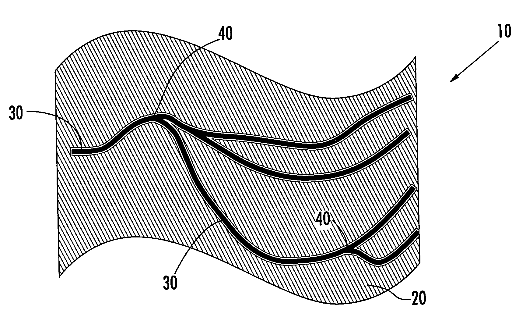
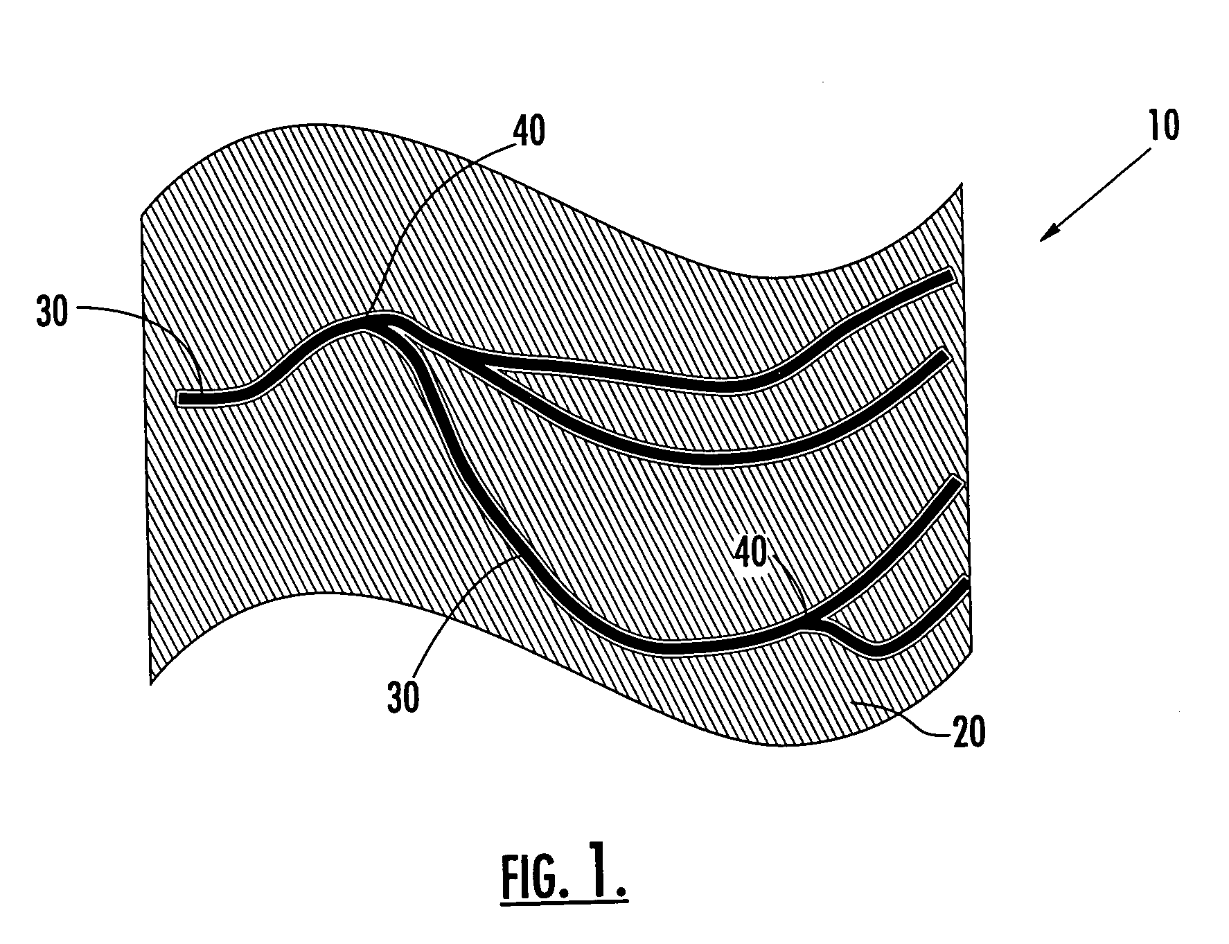
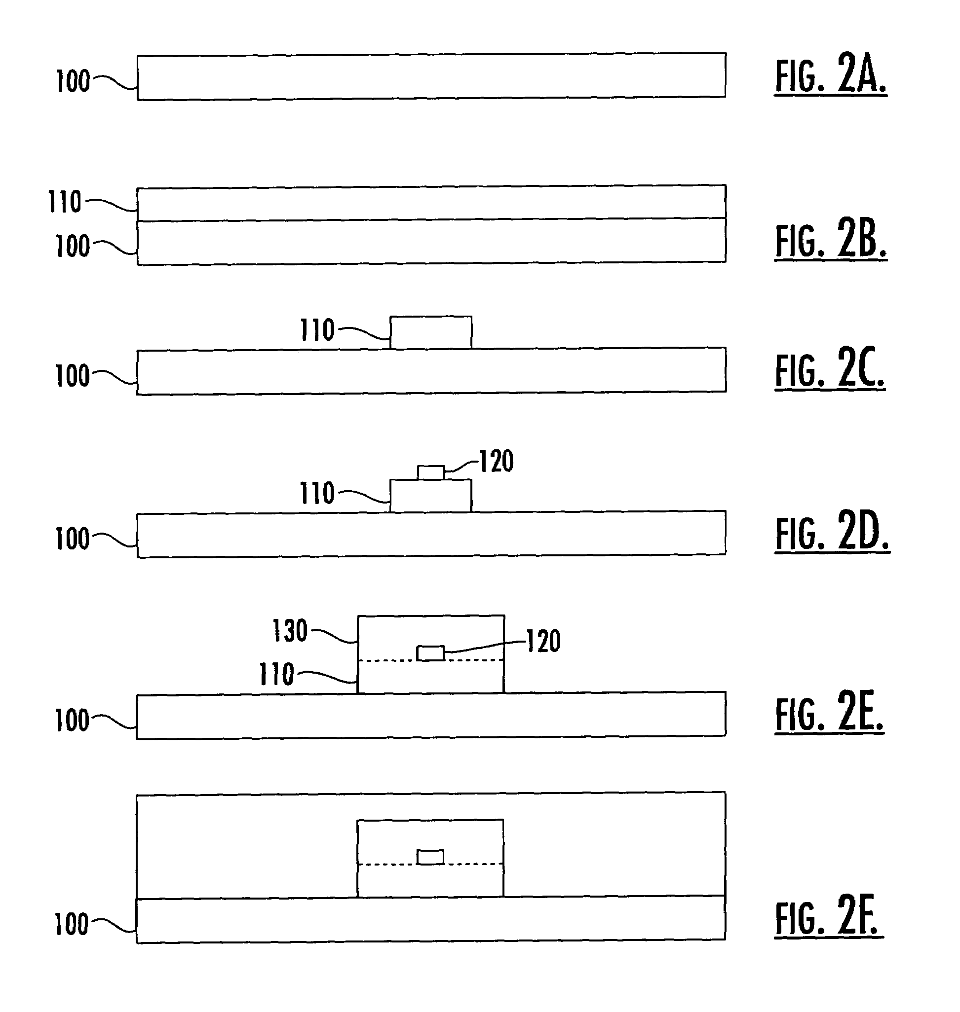
[0051]The invention as disclosed includes numerous embodiments of novel optical interconnect (i.e. waveguide) devices and associated optical devices that include these optical interconnects. In addition, the invention incorporates the methods for fabricating the material used to form the interconnects, the fabrication of the interconnects and methods for using the interconnects of the present invention.

Sol-Gel Based Waveguides Formed on Flexible Substrates...


PUM

PropertyMeasurementUnit
Lengthaaaaaaaaaa
Lengthaaaaaaaaaa
Lengthaaaaaaaaaa

Abstract

An optoelectronic device having a flexible substrate and an optical interconnect (i.e. waveguide) comprising a sol-gel based material formed on the substrate. The sol-gel based waveguide is capable of being integrated into an all-optical system and provides for greater interconnect distance and lower signal loss. Other sol-gel based optical devices, such as filters, optical source, detectors, sensors, switches and the like, will be implemented in conjunction with the sol-gel based waveguides to provide for an integrated optical system. Methods of formulating the sol-gel based material and methods for fabricating the sol-gel based devices are also provided.

Description

CROSS-REFERENCE TO RELATED APPLICATIONS[0001]The present application claims priority from U.S. Provisional Patent Application Ser. No. 60 / 194,663, entitled “Integrated Optical Circuits”, filed on Apr. 4, 2000, the contents of which are incorporated by reference.FIELD OF THE INVENTION[0002]The present invention relates to integrated optical circuits and more particularly to devices and systems that integrate sol-gel based optical interconnects with associated optical elements and methods for fabricating integrated sol-gel based optical interconnects.BACKGROUND OF THE INVENTION[0003]Advances in optical sciences have recently been widely recognized for their impact in the field of communications. These advances have precipitated innovation towards an all-optical network, which includes; sources, modulators, wavelength division multiplexers, amplifiers and functional optical devices. Such an all-optical network would provide increased bandwidth. However, barriers still exist that preven...

Claims


Application Information

Patent Timeline
IPC IPC(8): G02B6/122G02B6/13G02B6/12G02B6/138G02B6/42G02B6/43H01S5/026H01S5/40
CPCG02B6/12002G02B6/1221G02B6/13G02B6/138G02B6/42G02B6/43C08G77/58G02B2006/12147G02B2006/12164H01S5/026H01S5/4031H01S5/4068G02B2006/12107
Inventor FARAHI, FARAMARZ
Owner GULA CONSULTING LLC
Why Eureka
Try Eureka