Display device and method of manufacturing the same

a technology of a display device and a manufacturing method, which is applied in the direction of solid-state devices, layered products, chemistry apparatuses and processes, etc., can solve the problems of inability to manufacture tft having a good electric characteristic as when formed on a glass substrate, the temperature of a process must be lowered, and the heat resistance of a plastic film is low, so as to achieve the effect of low heat resistan

Inactive Publication Date: 2006-06-13
SEMICON ENERGY LAB CO LTD
View PDF17 Cites 216 Cited by
  • Summary
  • Abstract
  • Description
  • Claims
  • Application Information

AI Technical Summary

Benefits of technology

[0010]In the present invention, the above-mentioned elements are formed on a peeling layer that comprises a silicon film (silicon germanium film may be used, too), and then the peeling layer is removed by using a gas containing halogen fluoride in a final process. As a result, the respective elements and the substrate are separated from each other. Thereafter, it becomes possible to adhere the elements on the plastic substrate. Since the etching of the silicon film by halogen fluoride readily proceeds at room temperature, the process can be performed without any problem after the formation of a lumi...

Problems solved by technology

However, the heat resistance of a plastic film is low, and therefore the highest temperature of a process must be lowered.
As a result, the present situation is that a TFT hav...

Method used


Image

  • Display device and method of manufacturing the same
  • Display device and method of manufacturing the same
  • Display device and method of manufacturing the same

Examples


embodiment 1

[Embodiment 1]

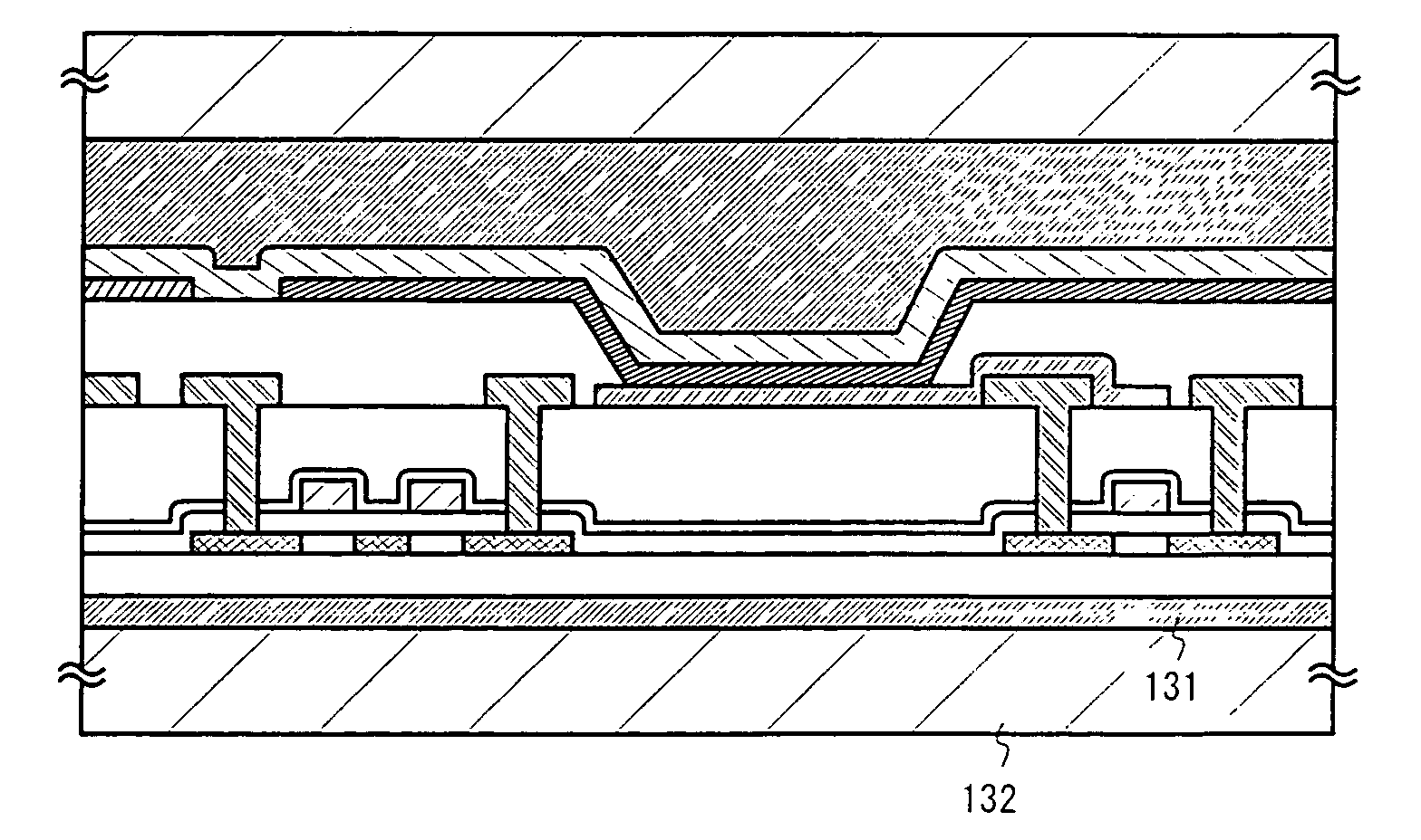
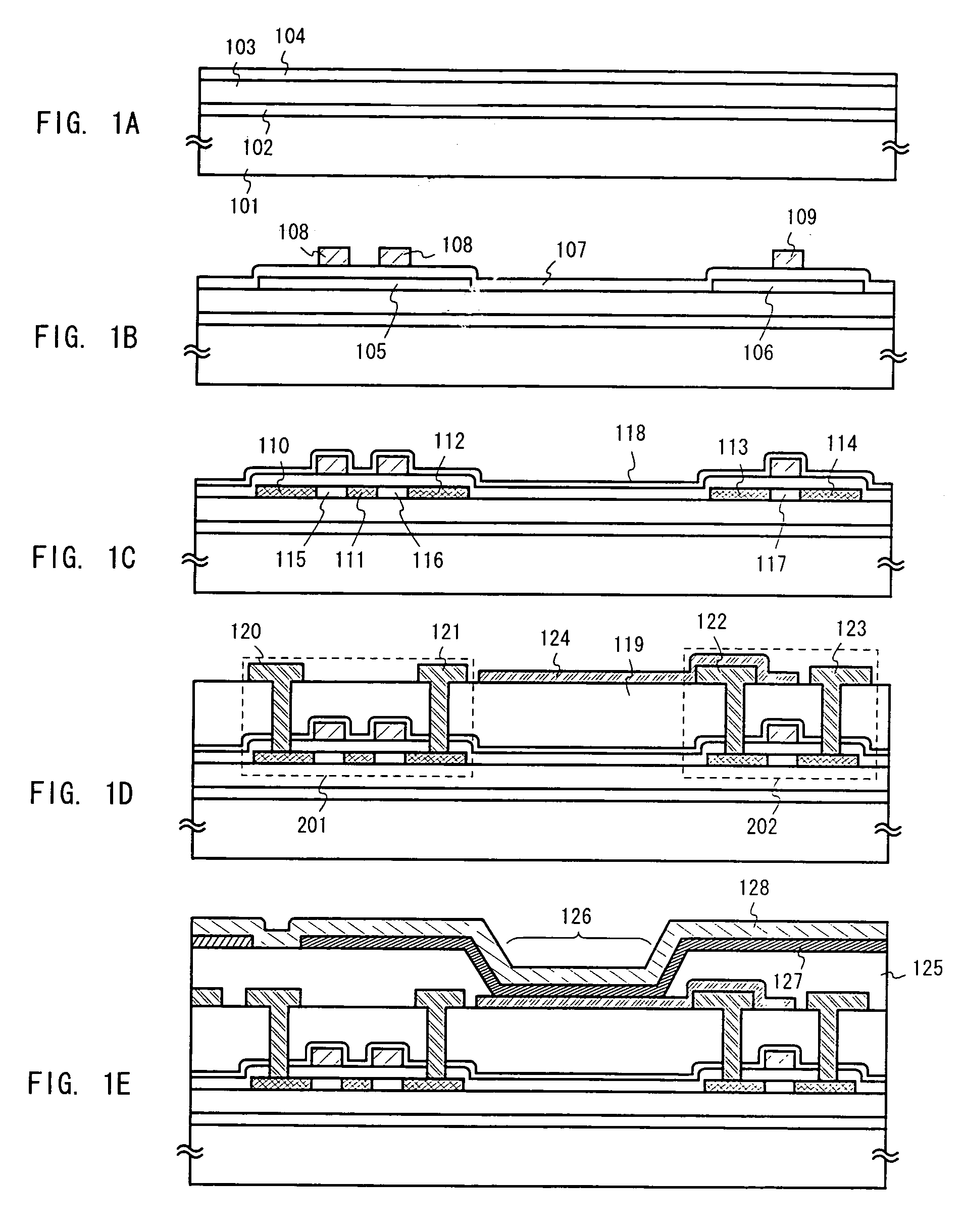
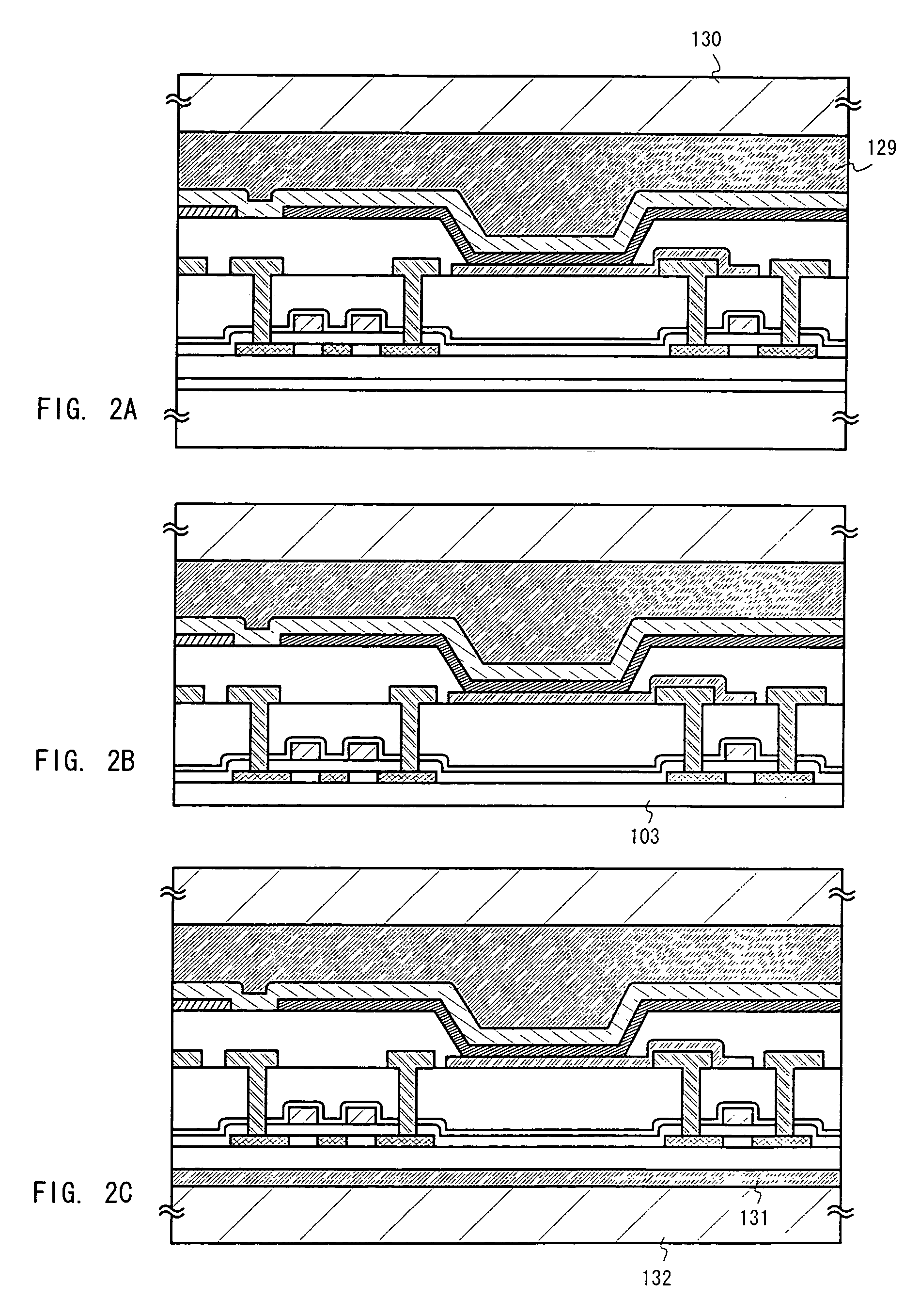
[0051]In Embodiment 1, an explanation will be made of an example of a case where an EL display device is manufactured by a method that is different from the one in the embodiment mode. The state shown in FIG. 1C is first obtained in accordance with the embodiment mode of the present invention. Then, after forming a silicon nitride film 118, a resist 401 is formed thereon. With the resist 401 as a mask, the silicon nitride film 118, a gate insulating layer 107, an insulating layer 103, and a peeling layer 102 are sequentially etched to thereby form opening portions 402 and 403 to reach an element-forming substrate 101. (See FIG. 4A)

[0052]Next, as shown in FIG. 4B, a first interlayer insulating layer 404 comprising resin is formed after the resist 401 is removed. A 2 μm thick polyimide film is used as the first interlayer insulating layer 404 in Embodiment 1. At this point, the element-forming substrate 101 and the first interlayer insulating layer 404 are bonded to each...

embodiment 2

[Embodiment 2]

[0063]In the embodiment mode or Embodiment 1 of the present invention, it is effective to employ any of the inventions disclosed in Japanese Patent Application Laid-open No. Hei 9-312260, Japanese Patent Application Laid-open No. Hei 10-247735, Japanese Patent Application Laid-open No. Hei 10-270363, and Japanese Patent Application Laid-open No. Hei 11-191628 by the present applicant for manufacturing processes up to the formation of the gate electrode.

[0064]All the techniques disclosed in the above-mentioned applications are techniques for forming a crystalline silicon film that has an extremely high crystallinity. Thus, TFTs having a very high performance may be formed by employing these techniques. Although heat treatment conducted at a temperature of 550° C. or more is included in any of these techniques, it becomes possible to use a low heat resistant plastic substrate as the element-forming substrate by employing the technique of the present invention.

[0065]It is...

embodiment 3

[Embodiment 3]

[0066]In Embodiment 3, an explanation will be made on an example of a case where the present invention is employed in a liquid crystal display device with reference to FIGS. 7A to 7C.

[0067]In FIG. 7A, reference symbol 701 denotes an element-forming substrate comprising glass, reference symbol 702 denotes a peeling layer comprising an amorphous silicon film, reference symbol 703 denotes an insulating layer comprising a silicon oxide nitride film, and reference symbol 704 denotes a pixel TFT. The pixel TFT 704 is a P channel TFT that is manufactured in accordance with the processes explained in the embodiment mode. In Embodiment 3, the pixel TFT 704 will be used as a switching element for controlling a voltage applied to a liquid crystal. Further, reference symbol 705 denotes a pixel electrode formed from a transparent conductive film that is electrically connected to the pixel TFT 704.

[0068]The above described structure may be formed in accordance with the manufacturing...


PUM


Abstract

To provide a technique for manufacturing a high-performance display device by employing a plastic substrate. A peeling layer is formed on an element-forming substrate, and a semiconductor element and a luminous element are further formed thereon. Then, a fixed substrate (130) is bonded on the luminous element by using a first adhesive (129). The entire substrate in this state is exposed in a gas containing halogen fluoride to thereby remove the peeling layer and separate the element-forming substrate. Thereafter, a bonding substrate (132) that comprises a plastic substrate is bonded in place of the separated element-forming substrate.

Description

BACKGROUND OF THE INVENTION[0001]1. Field of the Invention[0002]The present invention relates to a method of manufacturing a device having an element (hereinafter referred to as luminous element) that is comprised of a luminous material sandwiched between electrodes (the device will hereinafter be referred to as light-emitting device), or to a device having an element (hereinafter referred to as liquid crystal element) that is comprised of a liquid crystal sandwiched between electrodes (the device will hereinafter be referred to as liquid crystal display device). Note that a display device herein is a generic term referring to a light-emitting device and a liquid crystal display device.[0003]2. Description of the Related Art[0004]In recent years, development is proceeding in a light-emitting device (also called as a light-emitting diode or an EL display device) using a luminous element (hereinafter referred to as EL element) that utilizes a luminous material in which EL (Electro Lum...

Claims


Application Information

Patent Timeline
IPC IPC(8): B32B38/10H01L21/77H01L21/84H01L27/32H01L51/00H01L51/40
CPCH01L27/1214H01L27/1266H01L27/3244H01L27/322H01L27/3283Y10T156/1189H01L51/524H01L2227/326Y10S438/977Y10S156/924H01L51/0001H10K59/38H10K59/12H10K59/173H10K71/00H10K50/841H10K71/80H10K59/1201
Inventor YAMAZAKI, SHUNPEINAKAJIMA, SETSUO
Owner SEMICON ENERGY LAB CO LTD
Why Eureka
Try Eureka