

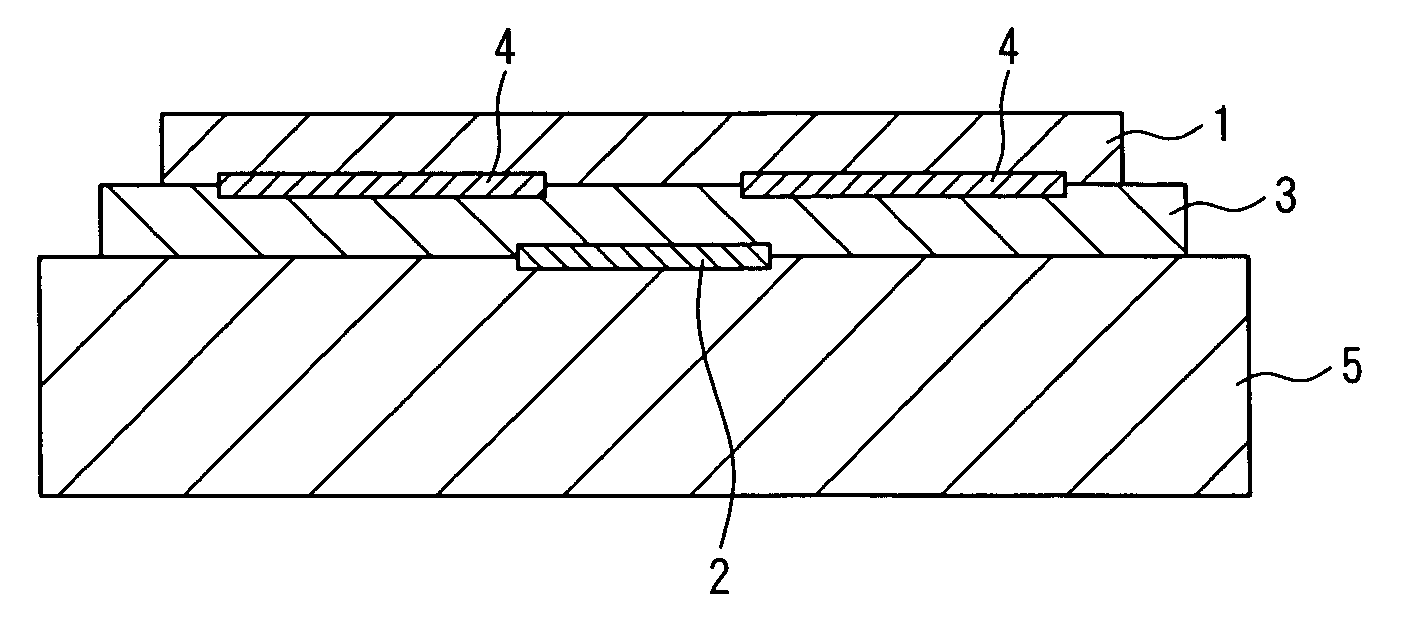
Organic semiconductor element
a technology of organic semiconductors and semiconductor elements, applied in thermoelectric devices, polycrystalline material growth, crystal growth process, etc., can solve the problems of limited size of use devices and remained non-reacted parts, so as to improve the speed of manufacturing transistors, reduce equipment space, and reduce the effect of cos
- Summary
- Abstract
- Description
- Claims
- Application Information
AI Technical Summary
Benefits of technology
Problems solved by technology
Method used
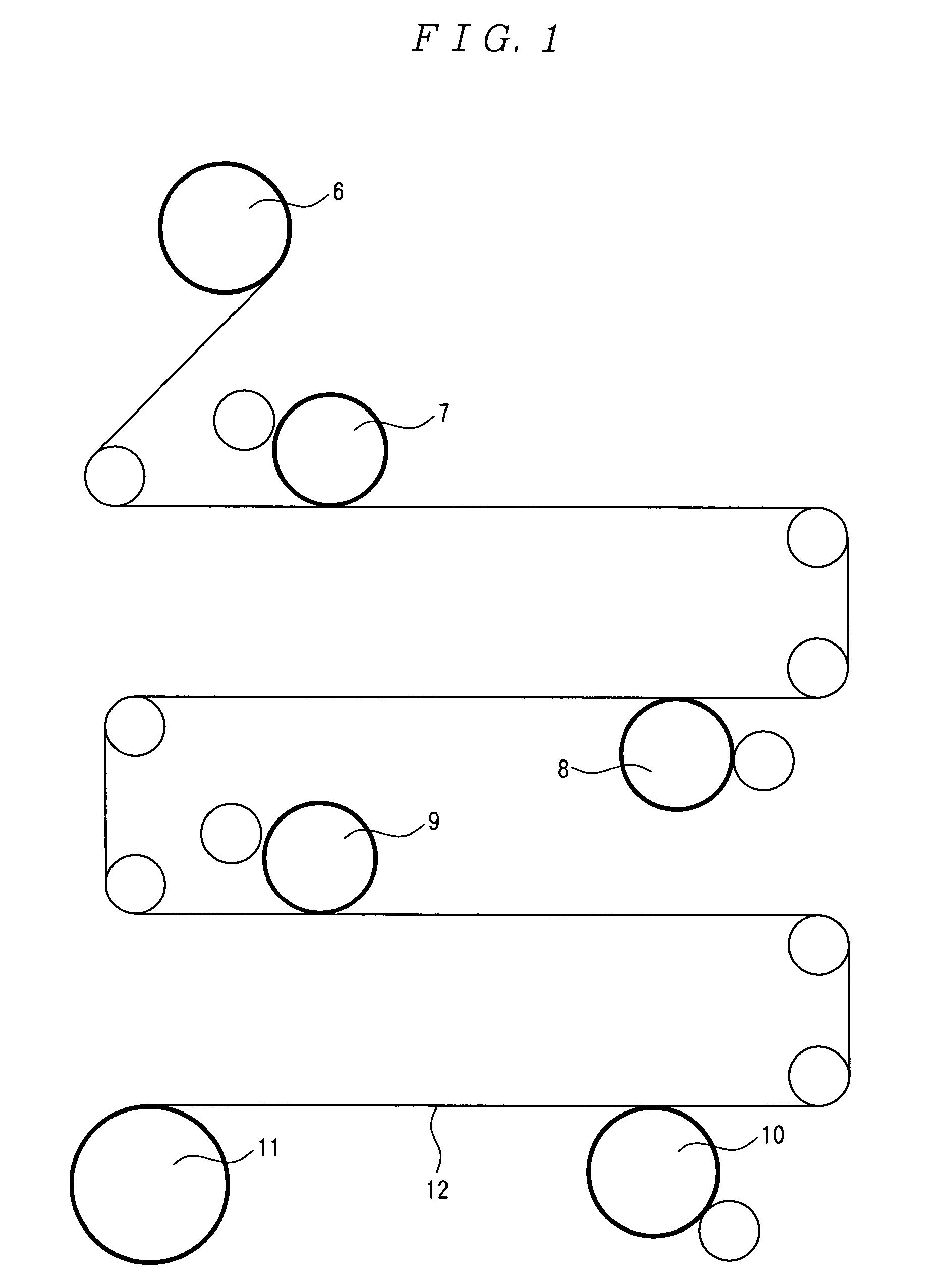
Image

Examples
example 1
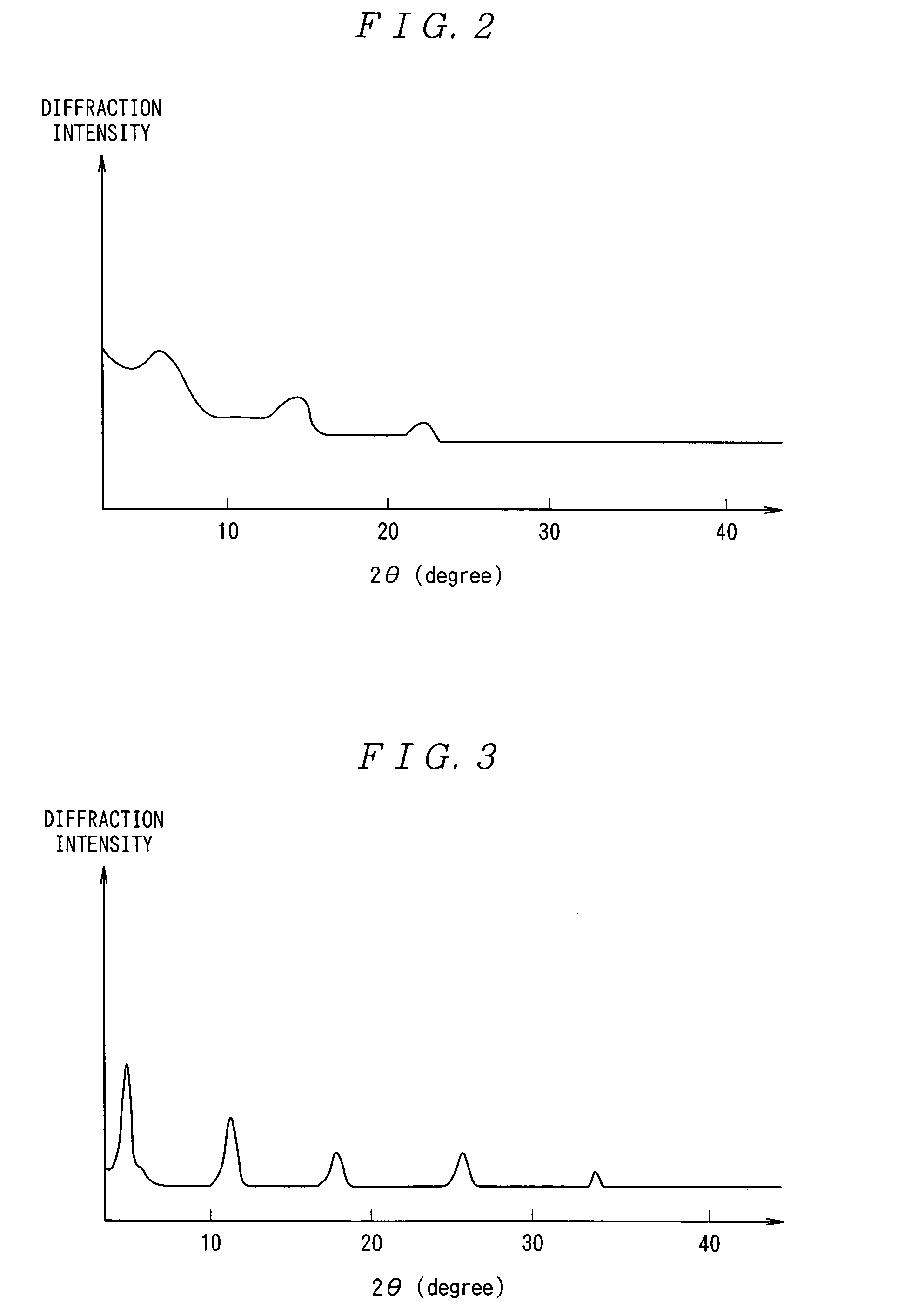
[0123]Naphthacene was dissolved in o-dichlorobenzene to prepare a solution (5% by mass) of naphthacene. The solution was cast onto a glass substrate and dried, and a thin film 350 nm thick was prepared. The X-ray diffraction pattern (CuKαray) revealed peaks of the (00n) plane (n=1, 2 and 3) with a c-axis lattice constant of 1.3 nm (see FIG. 2), indicating a crystalline thin film.
example 2
[0124]Pentacene was dissolved in o-dichlorobenzene to prepare a solution (0.05% by mass) of pentacene. The solution was applied several times onto a glass substrate and dried, and a thin film 90 nm thick was prepared. X-ray diffraction was performed as in Example 1, and the X-ray diffraction pattern revealed peaks of the (00n) plane (n=1, 2, 3, 4 and 5) with a c-axis lattice constant of 1.5 nm (see FIG. 3), indicating a crystalline thin film.
example 3
[0125]For hexacene, the method in literature (Minakata et al., Polymer Advanced Technology, 5, p602 (1995)) was employed. In short, naphthalene dialdehyde was reacted with anthracene dihydroquinone in ethanol in the presence of alkali to prepare dihydroxyhexacenequinone. The dihydroxyhexacenequinone was reduced by lithium aluminum hydride to synthesize dihydrohexacene, and the dihydrohexacene was dehydrogenated by copper (I) oxide in the presence of palladium catalyst to produce hexacene. Then, crystalline powder of hexacene was obtained by sublimation purification.
[0126]The hexacene thus prepared was dissolved in o-dichlorobenzene to prepare a solution (0.05% by mass) of hexacene. In an inert atmosphere, the solution was applied several times onto a glass substrate and dried, and a thin film was prepared. X-ray diffraction was performed as in Example 1, and the X-ray diffraction pattern revealed peaks of the (00n) plane (n=2 and 3) with a lattice constant of 1.8 nm, indicating a cr...
PUM
| Property | Measurement | Unit |
|---|---|---|
| carrier mobility | aaaaa | aaaaa |
| carrier mobility | aaaaa | aaaaa |
| temperature | aaaaa | aaaaa |
Abstract
Description
Claims
Application Information