Method of forming dual damascene metal interconnection employing sacrificial metal oxide layer

a metal interconnection and sacrificial metal technology, applied in the field of semiconductor devices, can solve the problems of etch damage, lack of process margins of vfdd photolithography process, and difficulty in forming photoresist patterns having an appropriate pitch just with exposure steps using krf lasers, etc., to achieve the effect of improving process margins

Active Publication Date: 2006-06-20
SAMSUNG ELECTRONICS CO LTD
View PDF8 Cites 11 Cited by
  • Summary
  • Abstract
  • Description
  • Claims
  • Application Information

AI Technical Summary

Benefits of technology

[0013]Therefore, the present invention provides a method of forming a dual damascene metal interconnection, the method being improving process margins of a photolithography process and an etch process together for the formation of a trench, without requiring an additional process for aligning a via hole and a trench.
[0018]In one embodiment, a capping layer may be further formed on the sacrificial metal oxide layer. The capping layer functions to reduce a reflectivity of the sacrificial metal oxide layer, and improve a capability of controlling a CD and a CD uniformity. The capping layer is preferably formed to have a thickness of 100 Å to 500 Å. Further, while patterning the sacrificial metal oxide layer, the capping layer may be patterned together to form a capping layer pattern. The capping layer pattern is preferably removed during the formation of the trench.
[0019]Preferably, before forming the interlayer insulating layer, an etch barrier layer may be formed. The etch barrier layer may include a silicon nitride (SiN) layer, a silicon carbide (SiC) layer, or a silicon carbon nitride (SiCN) layer. The etch barrier layer functions to prevent etch damages on the semiconductor substrate during the formation of the preliminary via hole.
[0021]Further, the sacrificial via protecting layer may be preferably formed of a spin on deposition (SOD) layer which is dry etched at a dry etch rate which is substantially identical to that of the interlayer insulating layer, and has a significantly high wet etch selectivity to the interlayer insulating layer. The SOD layer can fill the preliminary via hole even with a small deposition thickness, and has a good planarization characteristics thereby increasing a process margin of a photolithography process. Preferably, the SOD layer may be formed of a hydrogen-siloxane layer, an organo-siloxane layer, or an SOP (spin on polymer) layer, and more preferably, may be formed of HSQ (hydrogen silsequioxane) or MSQ (methyl silsequioxane).
[0023]Further, the sacrificial metal oxide layer may be formed with a thickness of 200 Å to 1,000 Å. As the thickness of the sacrificial metal oxide layer decreases, a process margin of a photolithography process for patterning the sacrificial metal oxide layer may increase.

Problems solved by technology

Metal interconnections are associated with problems such as RC delay, EM (electro-migration), or the like.
However, the VFDD process may provide a lack of process margins of a photolithography process, in comparison with a typical photolithography process of forming a via hole or a trench only.
Particularly, as a problem, there may be considered a process margin of a photolithography process of forming the trench after forming the via hole.
Further, etch damage may be caused_in the lower interconnection exposed through the via hole during the formation of the trench.
In the case that a design rule is 90 nm or less, it is difficult to form a photoresist pattern having an appropriate pitch just with an exposure step using a KrF laser.
Thus, a photolithography process using a KrF laser as above is led to a lack of process margins such as a resolution and a depth of focus (DOF).
As a result, an etch process of forming a trench using the photoresist pattern as an etch mask cannot provide desired process margins.
Therefore, the dual damascene process of forming a trench using the photoresist pattern as an etch mask by the method disclosed in U.S. Pat. No. 6,329,118 cannot ensure process margins of photolithography and etch processes at the same time, in the recent trends of highly-integrated semiconductor devices.

Method used


Image

  • Method of forming dual damascene metal interconnection employing sacrificial metal oxide layer
  • Method of forming dual damascene metal interconnection employing sacrificial metal oxide layer
  • Method of forming dual damascene metal interconnection employing sacrificial metal oxide layer

Examples


Embodiment Construction

[0030]The present invention will now be described more fully hereinafter with reference to the accompanying drawings, in which preferred embodiments of the invention are shown. In the drawings, the thickness of layers and regions are exaggerated for clarity.

[0031]FIG. 1 is a sequential flow chart illustrating a method of forming a dual damascene metal interconnection according to an embodiment of the present invention, and FIGS. 2 to 11 are sectional views illustrating a method of forming a dual damascene metal interconnection according to the sequential flow chart of FIG. 1.

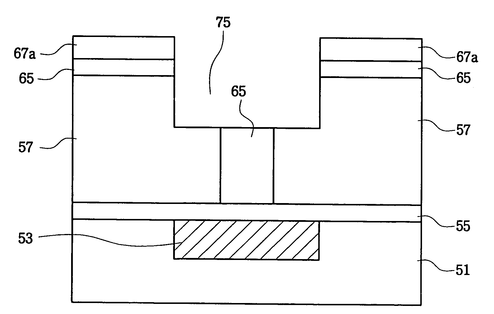
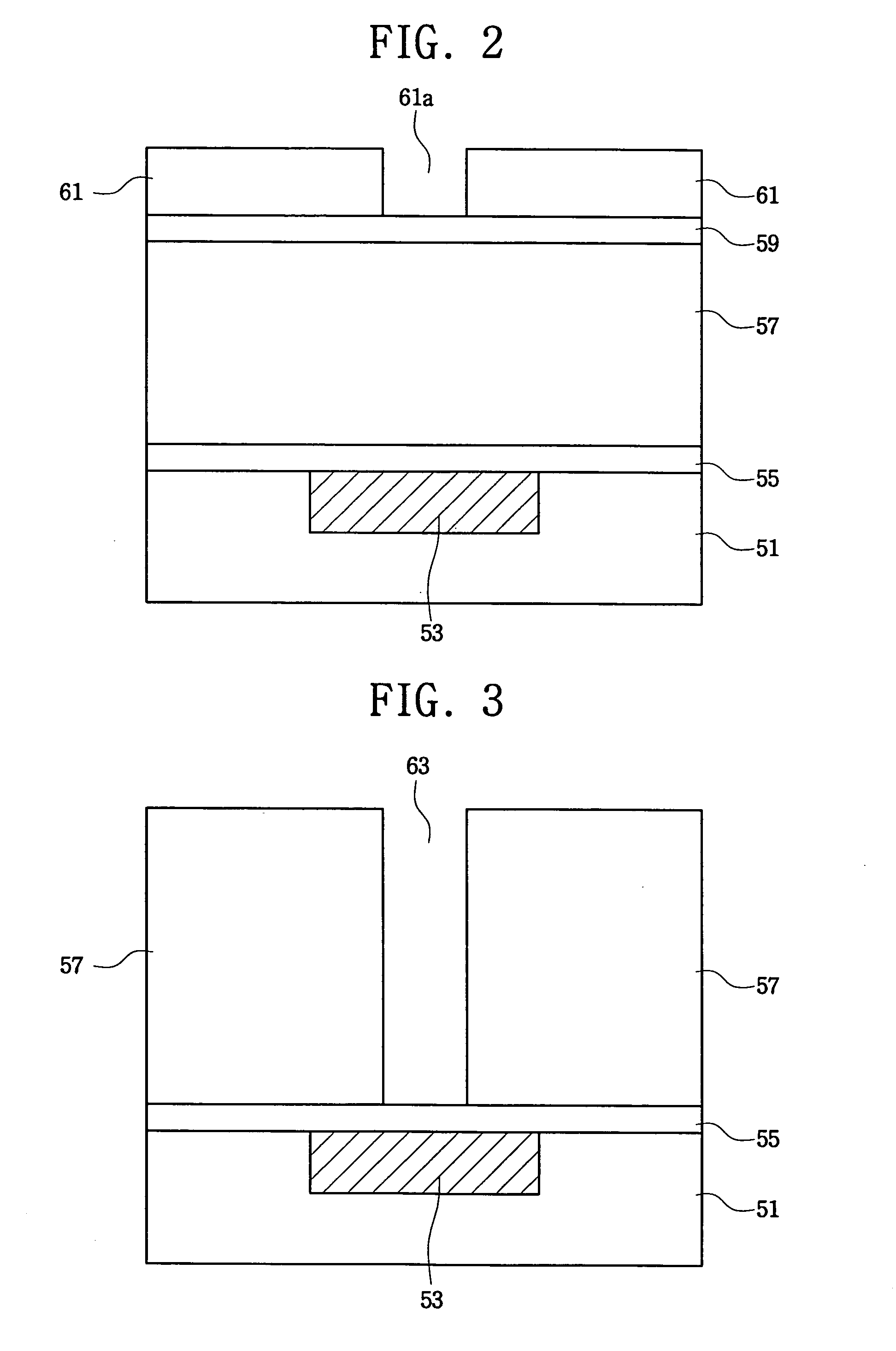
[0032]Referring to FIGS. 1 and 2, there is prepared a semiconductor substrate 51 having a lower interconnection 53 (step 1 of FIG. 1). The lower interconnection 53 may be formed using a damascene process. Further, the lower interconnection 53 may be a copper interconnection, and a diffusion barrier layer (not shown) may be formed on the side walls and the bottom of the copper interconnection 53.

[0033]Further, th...


PUM

PropertyMeasurementUnit
transparentaaaaaaaaaa
visible wavelengthaaaaaaaaaa
thicknessaaaaaaaaaa

Abstract

There is provided a method of forming a dual damascene metal interconnection by employing a sacrificial metal oxide layer. The method includes preparing a semiconductor substrate. An interlayer insulating layer is formed on the semiconductor substrate, and a preliminary via hole is formed by patterning the interlayer insulating layer. A sacrificial via protecting layer is formed on the semiconductor substrate having the preliminary via hole to fill the preliminary via hole, and cover an upper surface of the interlayer insulating layer. A sacrificial metal oxide layer is formed on the sacrificial via protecting layer, the sacrificial metal oxide layer is patterned to form a sacrificial metal oxide pattern having an opening crossing over the preliminary via hole, and exposing the sacrificial via protecting layer. The sacrificial via protecting layer and the interlayer insulating layer are etched using the sacrificial metal oxide pattern as an etch mask to form a trench located inside the interlayer insulating layer.

Description

CROSS-REFERENCE TO RELATED APPLICATION[0001]This application claims the benefit of Korean Patent Application No. 2003-87351, filed on Dec. 3, 2003, the contents of which are hereby incorporated herein by reference in their entirety.BACKGROUND[0002]1. Technical Field[0003]The present invention relates to a method of forming semiconductor devices, and more particularly, to a method of forming a dual damascene metal interconnection employing a sacrificial metal oxide layer.[0004]2. Discussion of the Related Art[0005]With the increase of integration degrees of semiconductor devices, the process of metal interconnection fabrication is becoming increasingly important in affecting reliability of semiconductor devices. Metal interconnections are associated with problems such as RC delay, EM (electro-migration), or the like. As one of the methods of solving the problems, a copper interconnection and a low-k dielectric layer are employed on a semiconductor device, and a damascene process is u...

Claims


Application Information

Patent Timeline
Patent Type & Authority Patents(United States)
IPC IPC(8): H01L21/4763H01L21/302H01L21/311H01L21/461H01L21/28H01L21/768
CPCH01L21/76808H01L21/31144H01L21/28
Inventor KIM, JAE-HAKMOON, YOUNG-JOONLEE, KYOUNG-WOOHWANG, JEONG-WOOK
Owner SAMSUNG ELECTRONICS CO LTD
Why Eureka
Try Eureka