Depositing layers in OLED devices using viscous flow

a technology of viscous flow and oled device, which is applied in the direction of electroluminescent light sources, vacuum evaporation coatings, coatings, etc., can solve the problems of direct contact with the surface of the substrate, abrasion, distortion, or partial lifting of the first-color pattern, and partial oxidative decomposition of the uniformly deposited organic ligh

Inactive Publication Date: 2006-06-27
GLOBAL OLED TECH
View PDF19 Cites 42 Cited by
  • Summary
  • Abstract
  • Description
  • Claims
  • Application Information

AI Technical Summary

Benefits of technology

[0041]A feature of the present invention is that the method of color pixelating an organic layer uses directed vapor beams of organic materials.
[0042]Another feature of the present invention is that the method of color pixelating an organic layer is effected in a chamber at reduced pressure and in the presence of an inert gas.
[0043]Another feature of the present invention is that the method of color pixelating an organic layer permits concurrent three-color patternwise deposition onto an OLED display substrate.
[0044]Another feature of the present invention

Problems solved by technology

The complexity of this process resides in the requirements that the integral shadow mask have multilevel topological features, which may be difficult to produce, and that angular positioning of the substrate with respect to one or more vapor sources must be controlled.
In general, positioning an element such as, for example, a donor sheet or a mask, in direct contact with a surface of a substrate can invite problems of abrasion, distortion, or partial lifting of a relatively thin and mechanically fragile organic layer which has been formed previously on the substrate surface.
In depositing a second-color pattern, direct contact of a donor sheet or a mask with the first-color pattern may cause abrasion, distortion, or partial lifting of the first-color pattern.
However, the ink-jet printing of dopants is performed under ambient conditions in which oxygen and moisture in the ambient air can result in partial oxidative decomposition of the uniformly deposited organic light-emitting layer containing the host material.
Additionally, direct diffusion of a dopant, or subsequent diffusion of a dopant, into the light-emitting layer can cause partial swelling and attendant distortion of the domains of the

Method used


Image

  • Depositing layers in OLED devices using viscous flow
  • Depositing layers in OLED devices using viscous flow
  • Depositing layers in OLED devices using viscous flow

Examples


Embodiment Construction

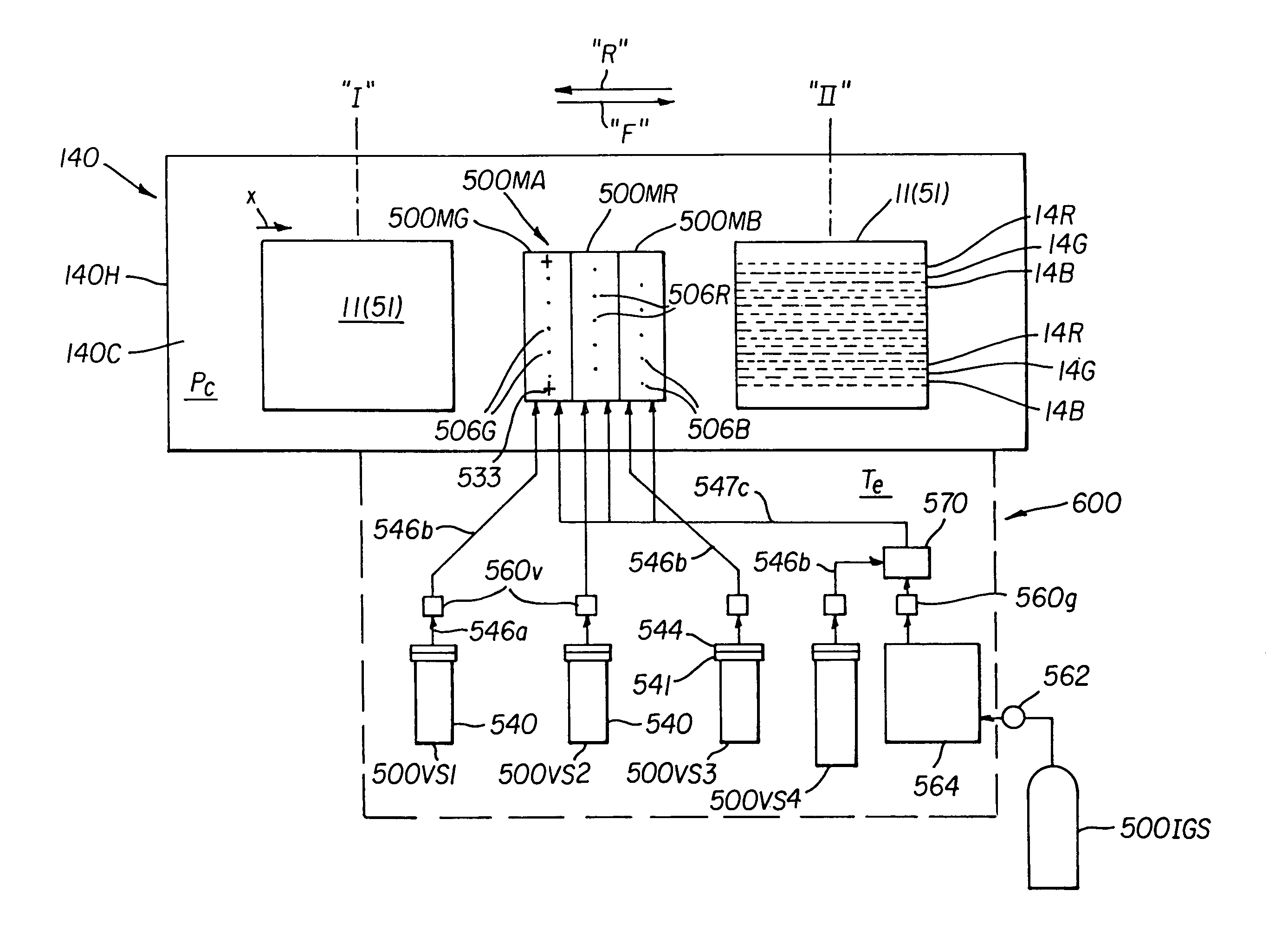
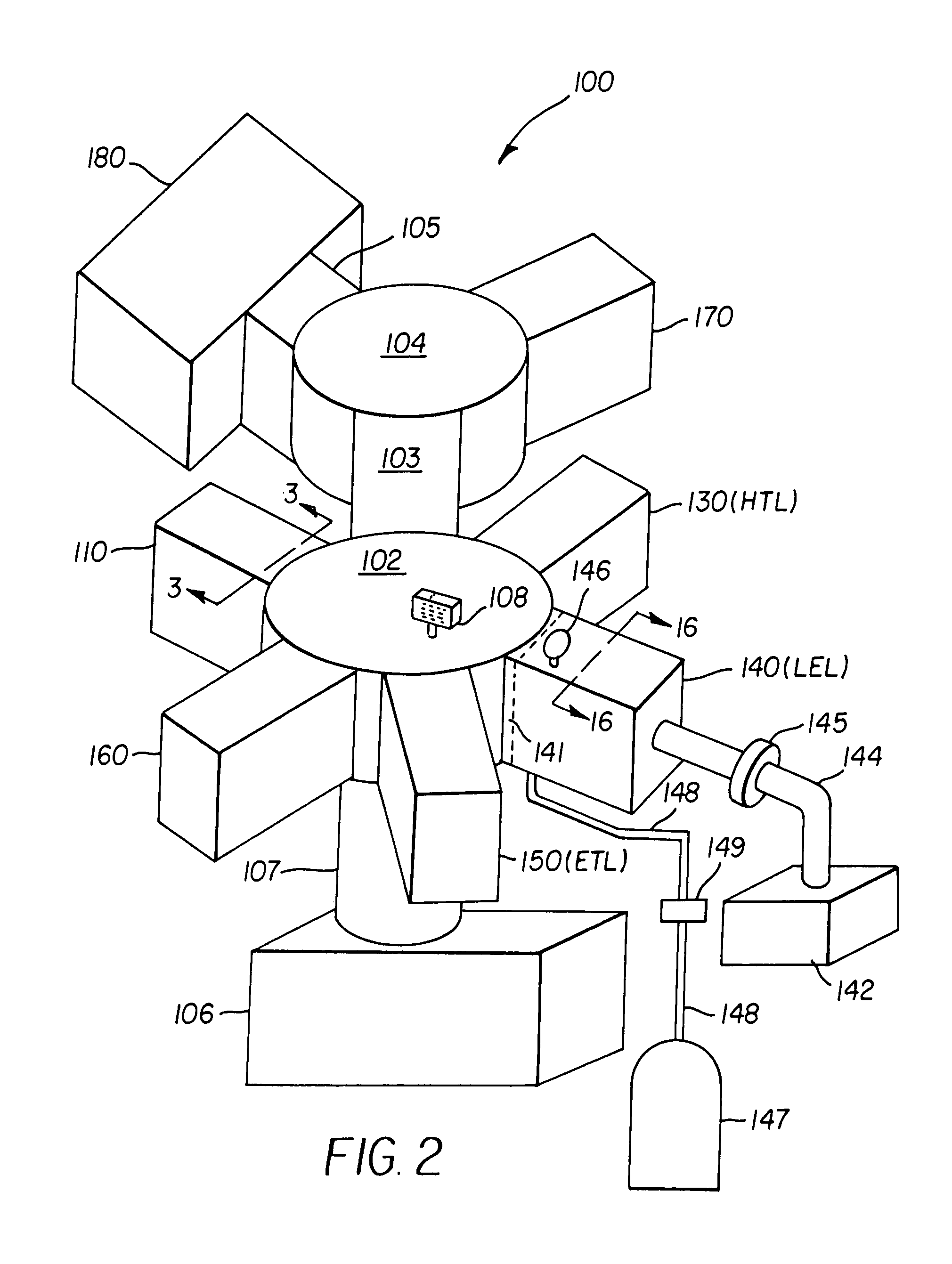
[0067]The drawings are necessarily of a schematic nature since layer thickness dimensions of OLEDs are frequently in the sub-micrometer ranges, while features representing lateral device dimensions can be in a range of 25–2000 millimeter. Furthermore, the plurality of nozzles formed in the nozzle plate(s) or structure(s) is relatively small in size when compared to a length dimension over which the nozzles extend. Accordingly, the drawings are scaled for ease of visualization rather than for dimensional accuracy.

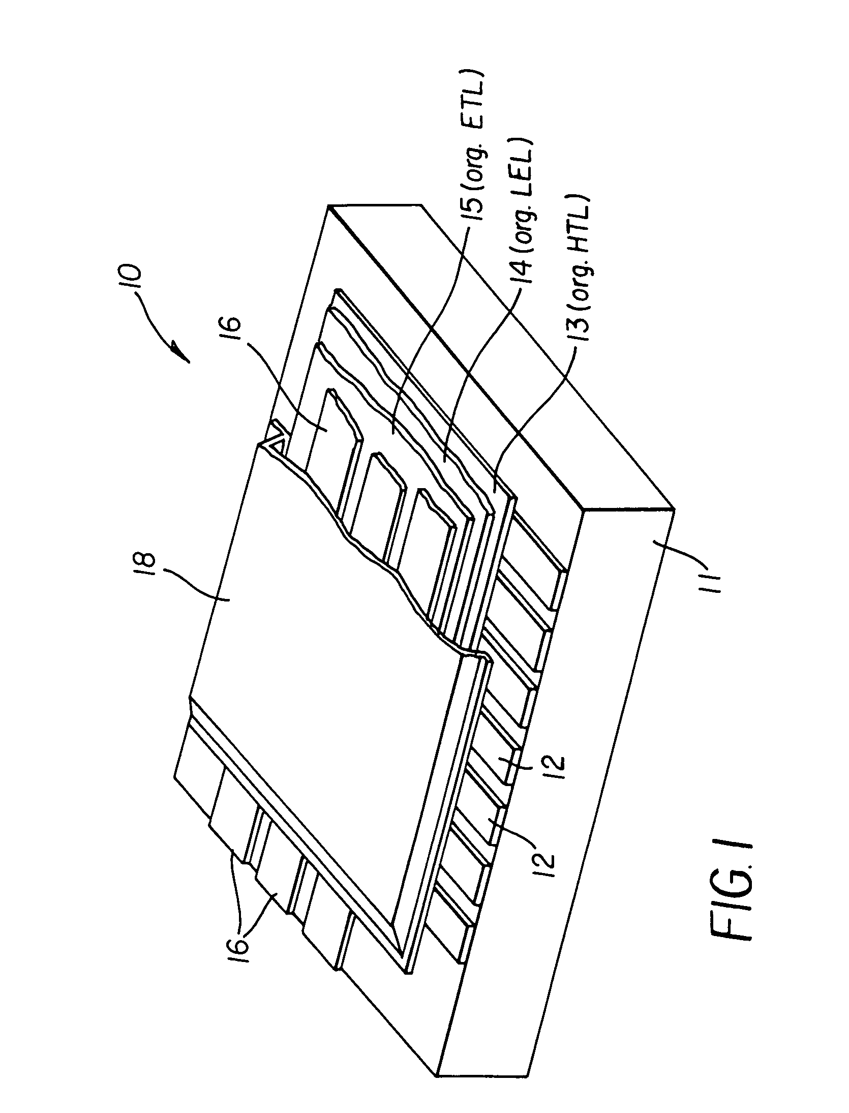
[0068]The term “display” or “display panel” is employed to designate a screen capable of electronically displaying video images or text. The term “pixel” is employed in its art-recognized usage to designate an area of a display panel that can be stimulated to emit light independently of other areas. The term “multicolor” is employed to describe a display panel that is capable of emitting light of a different hue in different areas. In particular, it is employed to describe a...


PUM

PropertyMeasurementUnit
Lengthaaaaaaaaaa
Distanceaaaaaaaaaa
Temperatureaaaaaaaaaa

Abstract

A method of depositing a patterned organic layer includes providing a manifold and an OLED display substrate in a chamber at reduced pressure and spaced relative to each other; providing a structure sealingly covering at least one surface of the manifold, the structure including a plurality of nozzles extending through the structure into the manifold. The method also includes delivering vaporized organic materials into the manifold, and applying an inert gas under pressure into the manifold so that the inert gas provides a viscous gas flow through each of the nozzles, such viscous gas flow transporting at least portions of the vaporized organic materials from the manifold through the nozzles to provide directed beams of the inert gas and of the vaporized organic materials and projecting the directed beams onto the OLED display substrate for depositing a pattern of an organic layer on the substrate.

Description

CROSS REFERENCE TO RELATED APPLICATIONS[0001]Reference is made to commonly assigned U.S. patent application Ser. No. 10 / 252,639 filed Sep. 23, 2002 now U.S. Pat. No. 6,911,671 by Michael A. Marcus et al., entitled “Device for Depositing Patterned Layers in OLED Displays”, the disclosure of which is herein incorporated by reference.FIELD OF THE INVENTION[0002]The present invention relates to forming patterned organic layers in making a multicolor OLED display or full-color OLED display, and more particularly to vapor depositing such patterned layers without requiring precision shadow masks.BACKGROUND OF THE INVENTION[0003]An organic light-emitting diode (OLED) device, also referred to as an organic electroluminescent device, can be constructed by sandwiching two or more organic layers between first and second electrodes.[0004]In single-color OLED devices or displays, also called monochrome OLEDs, these organic layers are not patterned but are formed as continuous layers.[0005]In mult...

Claims


Application Information

Patent Timeline
IPC IPC(8): B05D5/06B05D5/12H05B33/10C23C14/24H01L27/32H01L51/00H01L51/30H01L51/40H01L51/50H01L51/56H05B33/12
CPCH01L51/0002H01L51/0003H01L51/0008H01L27/3211H01L51/56H01L51/0004H01L51/005H01L51/0052H01L51/0059H01L51/0062H01L51/0081H01L51/0084H01L51/0085H01L51/0089H01L27/3281H10K59/35H10K59/17H10K71/10H10K71/13H10K71/16H10K71/12H10K85/60H10K85/649H10K85/615H10K85/631H10K85/341H10K85/351H10K85/324H10K85/342H10K71/00H05B33/10
Inventor MARCUS, MICHAEL A.GRACE, JEREMYKLUG, JUSTIN H.VAN SLYKE, STEVEN A.
Owner GLOBAL OLED TECH
Why Eureka
Try Eureka