Dynamically variable field shaping element

a dynamic field and shaping element technology, applied in the field of electrochemical treatment, can solve the problems of exacerbated problems, difficult or impossible to obtain these properties in seed layers, and inability to meet the thickness irregularities of prior art electroplating techniques, and achieve uniform current distribution

Inactive Publication Date: 2006-07-04
NOVELLUS SYSTEMS
View PDF6 Cites 85 Cited by
  • Summary
  • Abstract
  • Description
  • Claims
  • Application Information

AI Technical Summary

Benefits of technology

[0022]The present invention helps to solve some of the problems outlined above by providing a time variable field shaping element, i.e., a mask or shield, that is placed in the electrochemical reactor to compensate for the poten...

Problems solved by technology

Prior art electroplating techniques are susceptible to thickness irregularities.
It is difficult or impossible to obtain these properties in seed layers having a thickness greater than about 120 nm to 130 nm.
The electroplating process will exacerbate any problems that exist with the initial seed layer due to increased deposition rates in thicker areas that are better able to conduct electricity.
The electroplating process must be properly controlled or else thickness of the layer will not be uniform, there will develop poor step coverage, and necking of embedded structures can lead to the formation of gaps of pockets in the embedded structure.
Due to these factors in combination, the range of current densities in which void free filling can be obtained over the entire wafer is limited.
While t...

Method used


Image

  • Dynamically variable field shaping element
  • Dynamically variable field shaping element
  • Dynamically variable field shaping element

Examples


Embodiment Construction

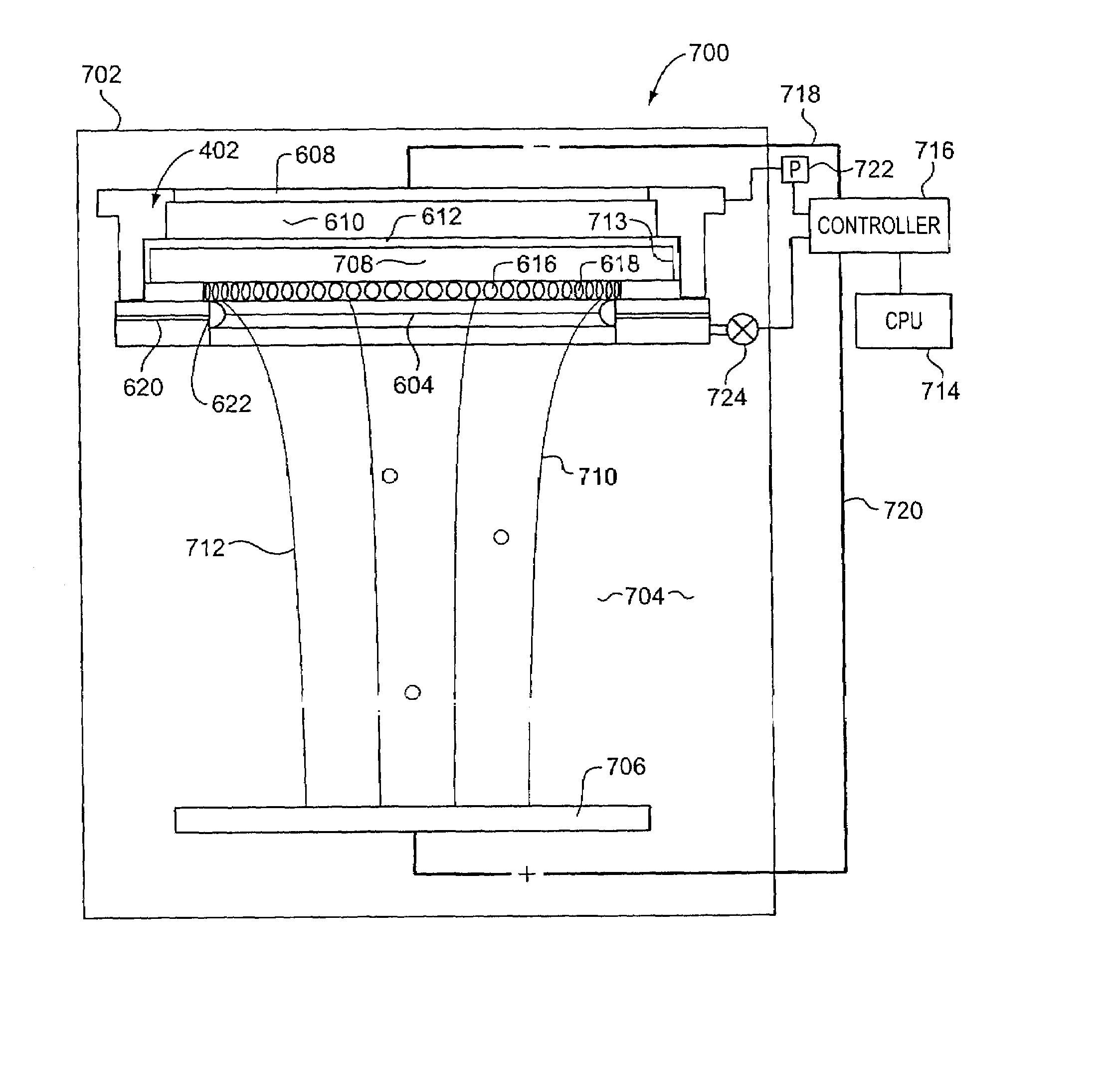
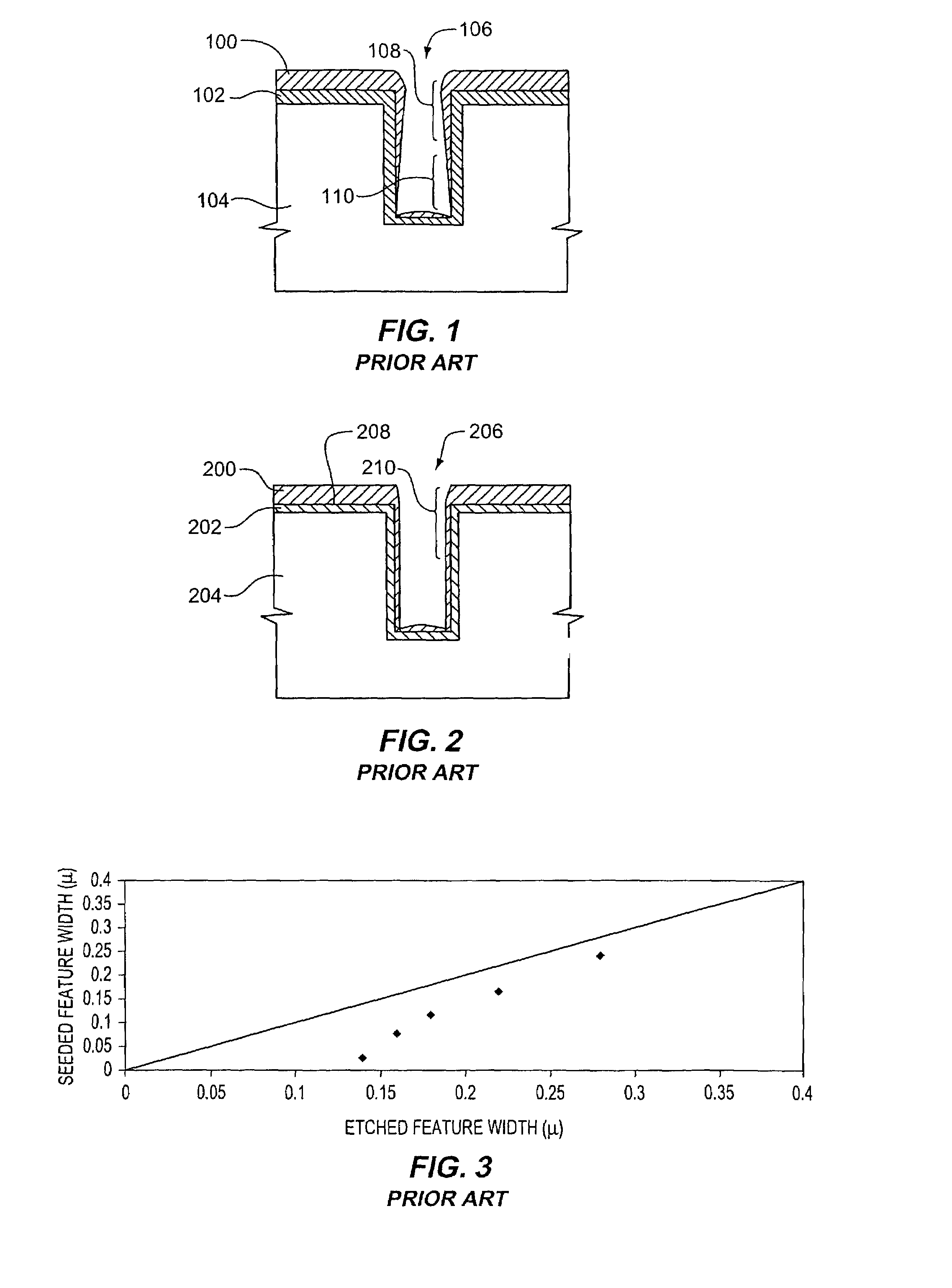
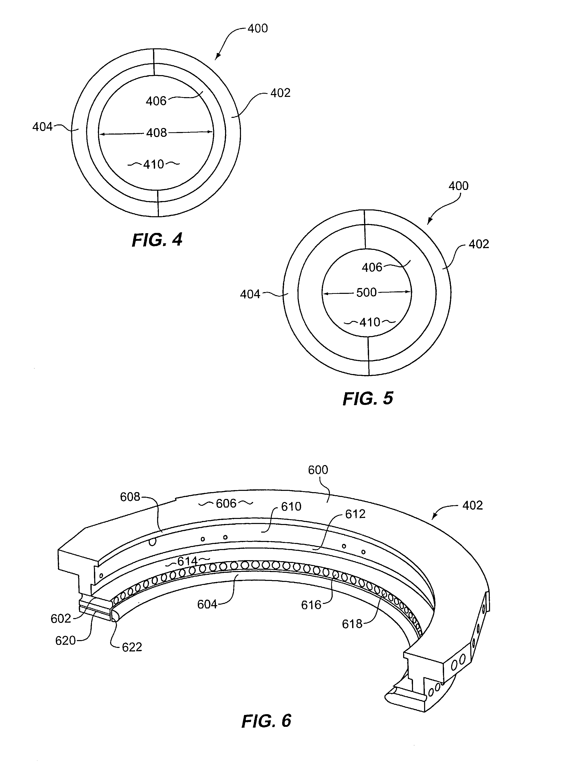
[0048]The invention is described herein with reference to FIGS. 1–14. It should be understood that the structures and systems depicted in schematic form in FIGS. 4–14 are used to explain the invention and are not precise depictions of actual structures and systems in accordance with the invention. Furthermore, the preferred embodiments described herein are exemplary and are not intended to limit the scope of the invention, which is defined in the claims below.

[0049]Embodiments in accordance with the invention compensate for electrical resistance and voltage drop across the wafer, particularly during phases of electrochemical treatment when the conductive metal film at the treatment surface of the substrate is especially thin; for example, at the beginning of an electroplating process when the thin seed layer dominates current flow and voltage drop, or in later stages of an electropolishing operation. Such compensation is generally conducted by shaping a potential drop in the electro...


PUM

PropertyMeasurementUnit
Thicknessaaaaaaaaaa
Angleaaaaaaaaaa
Sizeaaaaaaaaaa

Abstract

In an electrochemical reactor used for electrochemical treatment of a substrate, for example, for electroplating or electropolishing the substrate, one or more of the surface area of a field-shaping shield, the shield's distance between the anode and cathode, and the shield's angular orientation is varied during electrochemical treatment to screen the applied field and to compensate for potential drop along the radius of a wafer. The shield establishes an inverse potential drop in the electrolytic fluid to overcome the resistance of a thin film of conductive metal on the wafer.

Description

RELATED APPLICATIONS[0001]This application is a continuation-in-part application under 37 CFR 1.53(b) U.S. patent application Ser. No. 09 / 542,890 filed Apr. 4, 2000 now U.S. Pat. No. 6,514,393, which is hereby incorporated by reference. This application is also a continuation-in-part application under 37 CFR 1.53(b) of U.S. patent application Ser. No. 10 / 116,077 filed Apr. 4, 2002 now U.S. Pat. No. 6,755,954, which is hereby incorporated by reference and which is a continuation-in-part application of U.S. patent application Ser. No. 09 / 537,467 filed Mar. 27, 2000, which issued as U.S. Pat. No. 6,402,923 B1 on Jun. 11, 2002 to Mayer et al.FIELD OF THE INVENTION[0002]The present invention pertains to the field of electrochemical treatment and particularly to electroplating and electropolishing of integrated circuit substrate wafers and electronic memory storage devices, such as magnetic disks.BACKGROUND OF THE INVENTION[0003]Integrated circuits are formed on wafers by well-known proce...

Claims


Application Information

Patent Timeline
IPC IPC(8): C25D5/00C25D17/00C25D7/12C25D17/06
CPCC25D17/008C25D5/006C25D17/001C25D17/06C25D7/123C25D17/00C25F7/00
Inventor CONTOLINI, ROBERT J.MCCUTCHEON, ANDREW J.MAYER, STEVEN T.
Owner NOVELLUS SYSTEMS
Why Eureka
Try Eureka