Nitride semiconductor substrate and its production method

a technology of compound semiconductor substrate and semiconductor substrate, which is applied in the direction of polycrystalline material growth, crystal growth process, chemically reactive gas, etc., can solve the problems of large gan single crystals usable for practical applications, large gan single crystals, and inability to provide high-quality single crystals. , to achieve the effect of increasing the mass density of nitride semiconductors, reducing the number of defects, and high mass density

Active Publication Date: 2006-07-11
SUMITOMO CHEM CO LTD
View PDF7 Cites 11 Cited by
  • Summary
  • Abstract
  • Description
  • Claims
  • Application Information

AI Technical Summary

Benefits of technology

[0011]As a result of intense research in view of the above objects, the inventors have found that (a) in view of the fact that the level of large-area defects in crystals, such as impurities, nitrogen dissociation, polycrystals, voids, etc. can be found from the mass density of crystals or its distributions, a high-quality nitride semiconductor crystal with few defects can be obtained by increasing its mass density as an index to a desired level or more; that (b) a high mass density can be obtained by growing the nitride semiconductor with the partial pressure of a nitrogen compound gas kept sufficiently high; and that (c) a heat treatment in a nitrogen compound gas atmosphere after the growth of the nitride semiconductor can further increase the mass density of the nitride semiconductor. The present invention has been achieved based on these findings.

Problems solved by technology

However, because the sapphire base substrate has a different lattice constant from that of GaN, the direct growth of GaN on the sapphire base substrate fails to provide a single-crystal GaN layer.
However, even this method cannot remove the discrepancy of a lattice between a substrate and a crystal, resulting in GaN having numerous defects, which are expected to cause problems in the production of GaN laser diodes (LDs).
However, the above methods fail to provide high-quality, large GaN single crystals usable for practical applications.
For instance, because the ultra-high-temperature, high-pressure method needs pressures at several tens of thousands of atmospheres and temperatures at several thousands of degrees centigrade as growth conditions, it is difficult to produce large crystals.
The flux method suffers from problems such as nitrogen dissociation, the inclusion of fluxes of Na, Ca, etc. into crystals.
Also, because the control of the generation of nuclei is difficult at an early stage of growth, polycrystals are likely to be included in single crystals produced.
However, because of growth conditions causing a vigorous vapor phase reaction, foreign matters such as polycrystals, etc. are easily included in crystals generated, resulting in poor crystallinity.
Because these defects occurring in the crystals cause problems in the production of devices, they should be removed as much as possible.
However, because known evaluation means such as a transmission electron microscope (TEM), an X-ray diffraction (XRD), etc. evaluate the crystallinity of crystals extremely locally, it is difficult to evaluate the entire surfaces of large-area crystals obtained by actual crystal growth processes.
Therefore, it has so far been difficult to improve the characteristics of crystal substrates.

Method used


Image

  • Nitride semiconductor substrate and its production method
  • Nitride semiconductor substrate and its production method
  • Nitride semiconductor substrate and its production method

Examples


example 1

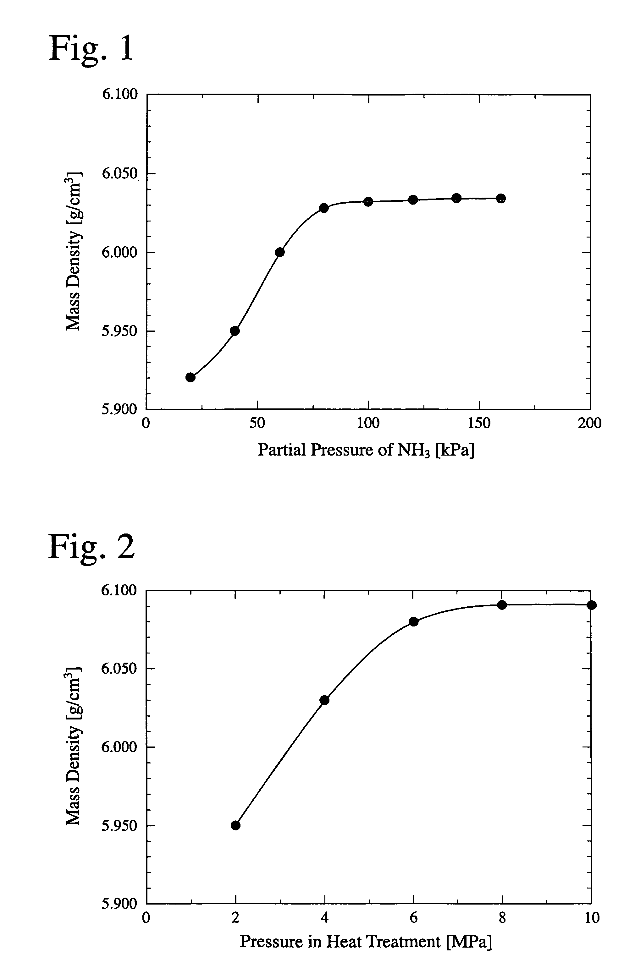
[0045]A 300-nm-thick GaN layer was formed on a 2-inch-diameter sapphire base substrate by a metal-organic vapor phase epitaxy (MOVPE) method. After Ti was vapor deposited on the GaN layer to a thickness of 20 nm, a heat treatment was conducted at 1000° C. for 30 minutes in a mixed atmosphere of H2 and NH3. The heat-treated substrate was charged into an HVPE furnace, in which GaN was grown to a thickness of 500 μm. Using GaCl and NH3 as starting materials of GaN, the partial pressure of NH3 was caused to change in a range of 20–160 kPa as shown in FIG. 1, with the partial pressure of GaCl fixed at 10 kPa. The resultant GaN layer was spontaneously separated from the sapphire base substrate. The resultant GaN plate was mirror-polished on both surfaces, to provide a 2-inch-diameter, 330-μm-thick, transparent, self-supported GaN substrate.

[0046]The mass density of the resultant self-supported GaN substrate measured by an Archimedes' method was, as shown in FIG. 1, 5.920–6.034 g / cm3, abou...

example 2

[0048]The self-supported GaN substrate having a mass density of 6.031 g / cm3, which was obtained in Example 1, was sealed in a high-pressure container, and heat-treated at 800° C. for 96 hours in an NH3 atmosphere. During the heat treatment, the pressure was changed in a range of 2–10 MPa, as shown in FIG. 2. The self-supported GaN substrate taken out of a furnace was measured with respect to a mass density by an Archimedes' method. As a result, its mass density was 5.950–6.090 g / cm3, about 98–100% of a theoretical mass density ρ (x). The results are shown in FIG. 2. In this Example, the effect of increasing a mass density by a heat treatment was obtained at a pressure higher than 4 MPa, and saturated substantially at about 8 MPa. Specifically, the mass density at 8 MPa was 6.085 g / cm3, about 99.9% of a theoretical mass density ρ (x), nearly 100%.

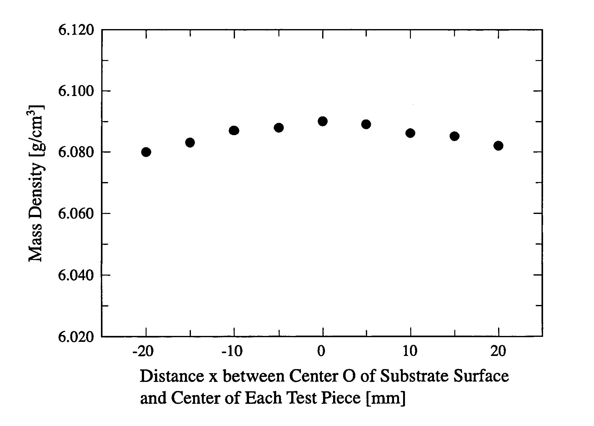
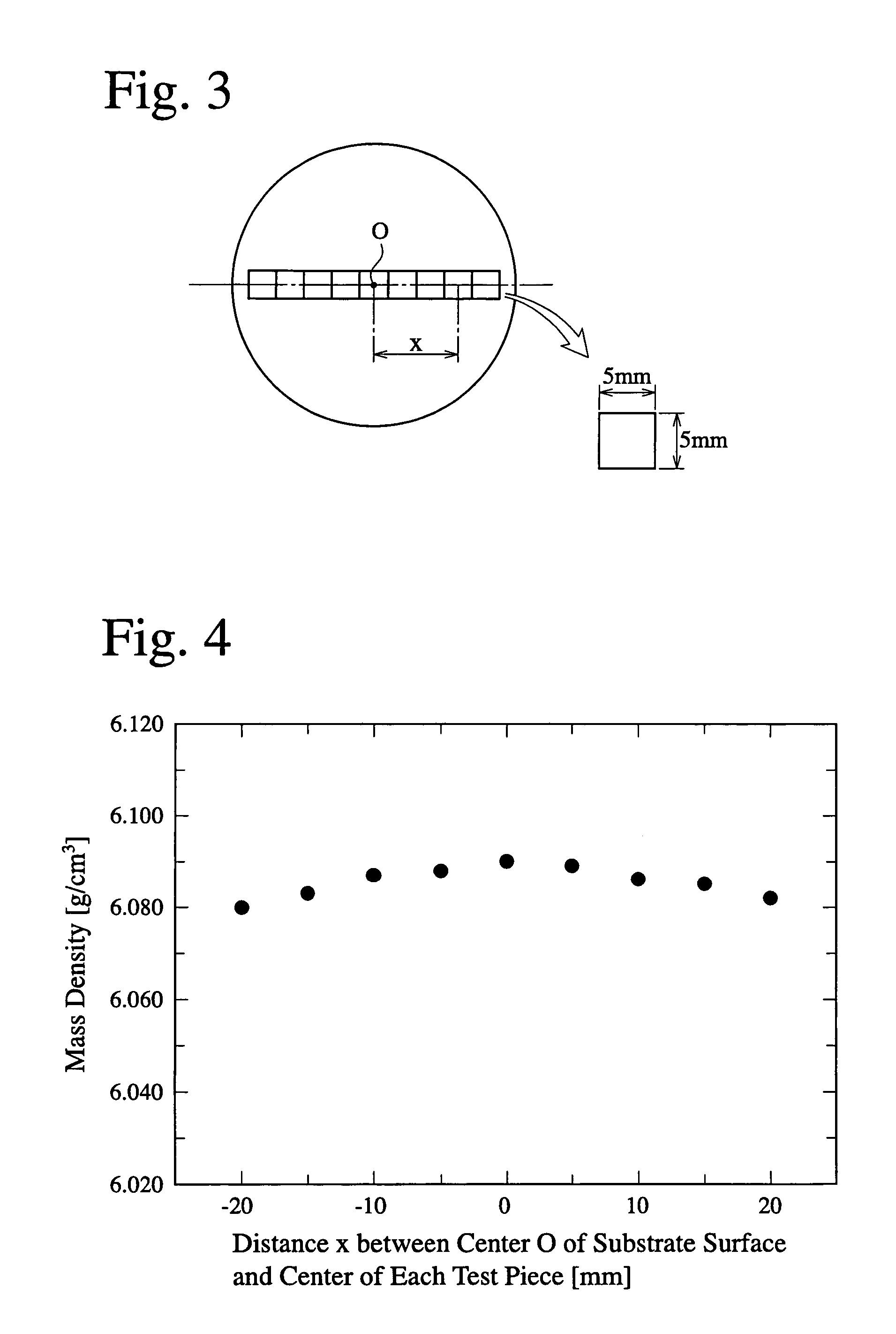
[0049]Test pieces of 5 mm each were cut out from the self-supported GaN substrate heat-treated at 8 MPa along its diameter, as shown in FIG...


PUM

PropertyMeasurementUnit
diameteraaaaaaaaaa
thicknessaaaaaaaaaa
partial pressureaaaaaaaaaa

Abstract

A nitride semiconductor substrate having a diameter of 10 mm or more, which has a single-layer structure composed of a nitride semiconductor layer having a basic composition represented by AlxGa1−xN (0≦x≦1), or a multi-layer structure comprising the nitride semiconductor layer, the mass density of the nitride semiconductor layer being 98% or more of a theoretical mass density ρ (x) represented by the following general formula (1):ρ⁡(x)=4⁢(Mx+MN)3⁢ax2⁢cx⁢Na,(1)wherein ax=aGaN+(aAlN−aGaN)x, wherein aGaN represents an a-axis length of GaN, and aAlN represents an a-axis length of AlN; cx=cGaN+(cAlN−cGaN)x, wherein cGaN represents a c-axis length of GaN, and CAlN represents a c-axis length of AlN; Mx=MGa+(MAl−MGa)x, wherein MGa represents the atomic weight of Ga, and MAl represents the atomic weight of Al; MN represents the atomic weight of nitrogen; and Na represents Avogadro's number.

Description

FIELD OF THE INVENTION[0001]The present invention relates to a nitride-type compound semiconductor substrate having a high mass density and a low defect density, and its production method.BACKGROUND OF THE INVENTION[0002]GaN compound semiconductors such as gallium nitride (GaN), indium gallium nitride (InGaN), aluminum gallium nitride (AlGaN), etc. are attracting much attention as materials for blue-ray light-emitting diodes (LEDs) and laser diodes (LDs). Particularly because GaN compound semiconductors have good heat resistance and environmental resistance, development has been conducted to apply them to electronic devices to utilize their characteristics.[0003]GaN-growing substrates widely used at present are sapphire base substrate. The production of GaN may be carried out generally by epitaxially growing GaN on a single-crystal sapphire base substrate by a metal-organic vapor phase epitaxy (MOVPE) method, etc.[0004]However, because the sapphire base substrate has a different lat...

Claims


Application Information

Patent Timeline
Patent Type & Authority Patents(United States)
IPC IPC(8): H01L29/15H01L29/12H01L31/0256C30B29/38C23C16/34C30B25/02C30B29/40H01L21/205H01L21/324H01L29/20
CPCH01L21/0242H01L21/0254H01L21/0262C30B29/40H01L21/3245H01L29/2003C30B25/02H01L21/02664
Inventor OSHIMA, YUICHI
Owner SUMITOMO CHEM CO LTD
Why Eureka
Try Eureka