Method of making active matrix substrate with pixel electrodes of photosensitive conductive material

a technology of photosensitive conductive material and active matrix substrate, which is applied in the direction of radiation control devices, identification means, instruments, etc., can solve the problems of affecting leakage failures, and hindering the photo resist of the attached area, so as to shorten the fabrication process of the pixel electrode and improve the exposure precision

Inactive Publication Date: 2006-07-11
SHARP KK
View PDF26 Cites 53 Cited by
  • Summary
  • Abstract
  • Description
  • Claims
  • Application Information

AI Technical Summary

Benefits of technology

[0015]Accordingly, it is an object of the present invention to provide an active matrix substrate which enables, by changing materials of a pixel electrode, to shorten the fabrication process of the pixel electrode, improve exposure precision by self alignment, and prevent leakage failures between the pixel electrodes, and to provide a display device and an image sensing device using the same.
[0027]In this case, using the gate signal lines and the source signal lines formed on the substrate as exposure masks and performing exposure from the back side of the substrate enable self-aligned pattern formation of film placed for the pixel electrodes and the like on the front side without practicing alignment. As a result, dispersion of parasitic capacitance, which is generated in a superposed portion of the pixel electrode and the gate signal line or in a superposed portion of the pixel electrode and the source signal line, can be uniformed in the entire pixel area, by which the uniformity of display is improved. In addition, a photosensitive conductive material applied over each signal line is not exposed unless any defect such as open holes are present on the signal lines. Accordingly, unlike the case of mask exposure of conventional positive type photo resist, a conductive film remain is not generated in clearance between pixel electrodes by the presence of dust in the process of exposure. Therefore, short-circuit between the pixel electrodes is not produced, which ensures insulation between the pixel electrodes.
[0029]In this case, the photosensitive conductive material can be formed easily. It is also advantageous that the photosensitive resin determining patterning conditions such as pre-bake temperature and light exposure and the conductive particles determining conductivity can be separately optimized.
[0033]Contrary to this, formation of a pixel electrode with a photosensitive conductive material containing color agents such as pigments allows the pixel electrode to function as a color filter as well. This eliminates necessity of forming a color filter on the opposite substrate side like the prior art. Consequently, any displacement, if it is generated between the substrates in the course of sticking the substrates together, will not decrease the aperture ratio of the pixel.

Problems solved by technology

However, the conventional active matrix substrate described hereinabove has following problems.
iii) In the process of patterning an ITO film, when positive type photo resist applied on the ITO film is mask-exposed, foreign matters such as dust attached on the substrate or on the mask hinder the photo resist of the attached area from being exposed, as a consequence of which the attached area is left as an unnecessary resist pattern.
If the unnecessary resist pattern is present in a clearance portion between adjacent pixel electrodes, the ITO film of the portion is not etched and remained in an etching step thereafter, which may establish electrical connection between the pixel electrodes, causing leakage failures.

Method used


Image

  • Method of making active matrix substrate with pixel electrodes of photosensitive conductive material
  • Method of making active matrix substrate with pixel electrodes of photosensitive conductive material
  • Method of making active matrix substrate with pixel electrodes of photosensitive conductive material

Examples


Embodiment Construction

[0045]The embodiments of the present invention will be described hereinafter with reference to drawings.

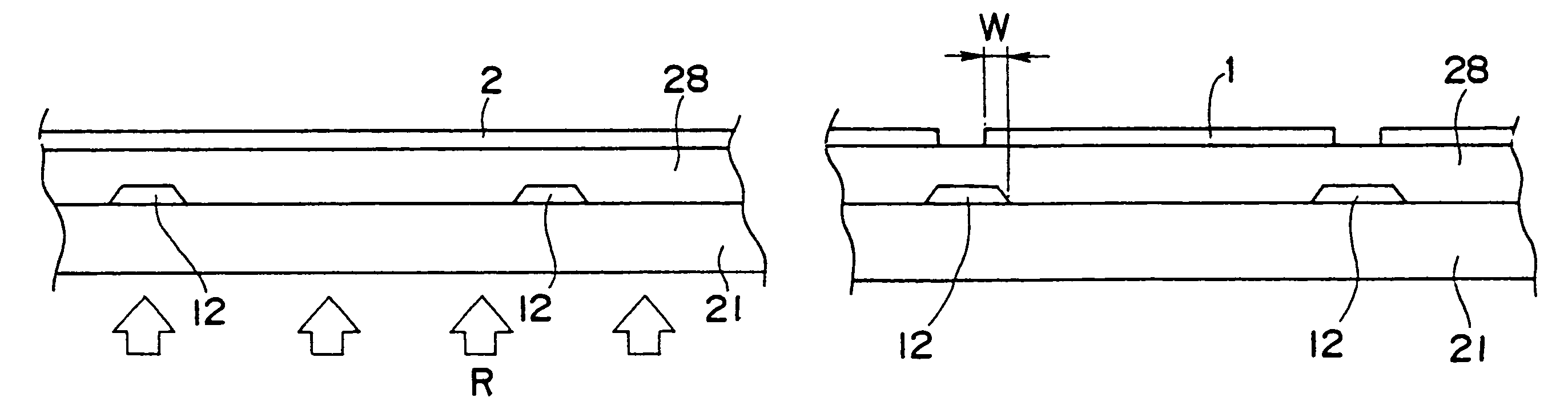
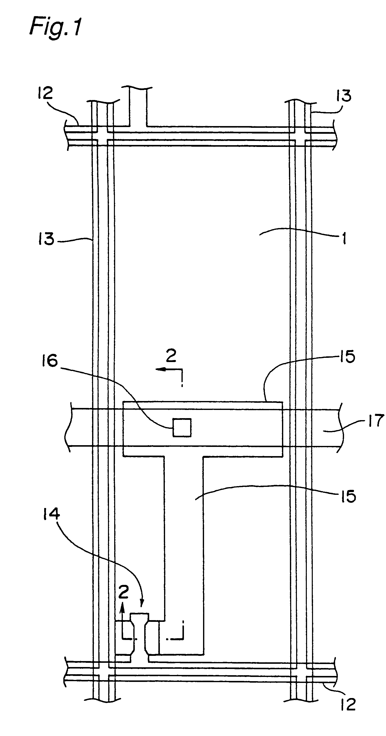
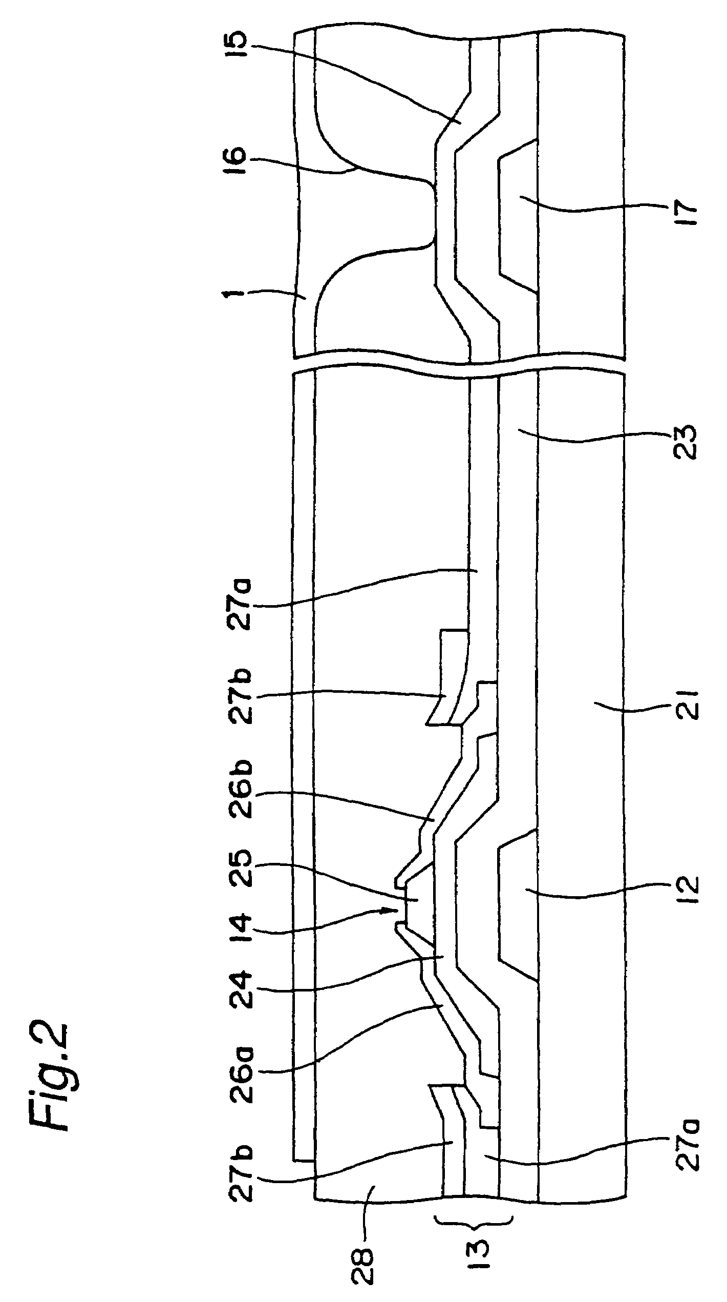
[0046]FIG. 1 is a plan view showing one pixel extracted from the pixels disposed in the shape of a matrix on an active matrix substrate as one example of the present invention, and FIG. 2 is a cross sectional view taken on the line 2—2 of FIG. 1. Except that the material and fabrication method of a pixel electrode is different, the active matrix substrate has the same configuration as the prior art shown in FIGS. 7 and 8, so that like component members are designated by like reference numerals.

[0047]The active matrix substrate is composed of: gate signal lines 12 placed on a light permeable substrate 21 along the lower side of a rectangle shown in the plan view and sending signals to a gate of a TFT 14; capacity lines 17 placed on the light permeable substrate 21 and positioned crosswise in the center of the rectangle of the plan view; a gate insulating film 23 covering the lines ...


PUM

PropertyMeasurementUnit
particle sizeaaaaaaaaaa
temperatureaaaaaaaaaa

Abstract

There is provided an active matrix substrate which enables to shorten a fabrication process of a pixel electrode, improve exposure precision by self alignment, and prevent leakage failures between pixel electrodes. On top of the interlayer insulating film, there are formed pixel electrodes, which are connected to the TFTs through contact holes piercing through the interlayer insulating film. The pixel electrodes are formed by applying on the interlayer insulating film a photosensitive transparent resin such as negative acrylic polymerized resin containing ITO, ATO or ZnO as transparent conductive particles, performing exposure from the back side of the substrate, and conducting development.

Description

[0001]This application is a divisional of U.S. Ser. No. 09 / 863,266, filed May 24, 2001 now abandoned, the disclosure of which is hereby incorporated herein by reference.BACKGROUND OF THE INVENTION[0002]The present invention relates to an active matrix substrate, and flat panel display device and image sensing device using the same.[0003]A liquid crystal display device, as is generally known, holds liquid crystal molecules in between two substrates on which electrodes are formed, and electric signals applied to between the electrodes on the both substrates vary the transmissivity of light coming from back light, by which information is displayed. Compared to cathode-ray tube display devices, the liquid crystal display devices are thin, light-weighted, and low power consumption, and mounted on such devices as desktop personal information terminal equipment and amusement instruments.[0004]As demands for high fineness and high image quality are increasing, a prevailing liquid crystal di...

Claims


Application Information

Patent Timeline
Patent Type & Authority Patents(United States)
IPC IPC(8): G02F1/1343G02F1/1362G02F1/1368G03F7/004G03F7/20G09F9/30H01L27/146
CPCG02F1/13439H01L27/14609G02F1/136227G02F1/1343
Inventor IZUMI, YOSHIHIROCHIKAMA, YOSHIMASA
Owner SHARP KK
Why Eureka
Try Eureka