
Programmable memory address and decode circuits with low tunnel barrier interpoly insulators

a technology of interpoly insulators and programmable memory addresses, which is applied in the field of integrated circuits, can solve the problems of large numbers of ttl integrated circuits typically required for a specific application, high cost of fabricating logic circuits tailored to and inability to meet the specific needs of a particular customer

Inactive Publication Date: 2006-07-11
MICRON TECH INC
View PDF120 Cites 74 Cited by
  • Summary
  • Abstract
  • Description
  • Claims
  • Application Information

AI Technical Summary

Benefits of technology

This solution enables faster write and erase speeds, reduces soft erase errors, and improves the reliability and yield of flash memory devices by lowering tunneling barriers and avoiding high electric fields, thus addressing the limitations of conventional interpoly dielectric insulators.

Problems solved by technology

Logic circuits that are tailored to the specific needs of a particular customer can be very expensive to fabricate on a commercial basis.
However, random logic circuits are still required to tie the various elements of a digital system together.
The drawback is that large numbers of TTL integrated circuits are typically required for a specific application.
This increases the consumption of power and board space, and drives up the overall cost of the digital system.
However, custom logic devices require significantly greater engineering time and effort, which increases the cost to develop these circuits and may also delay the production of the end system.
Essentially, at some point, the lithography cannot create a fine enough image with sufficient clarity to decrease the size of the elements of the circuit.
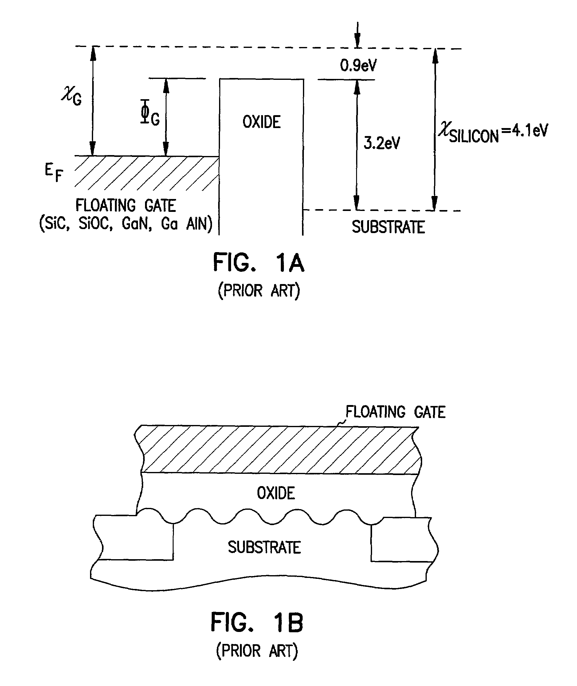
However, the rough top surface of the polysilicon floating gate resulted in, poor quality interpoly oxides, sharp points, localized high electric fields, premature breakdown and reliability problems.
However, in order to enable a reasonable write speed the ETOX cell uses channel hot electron injection, the erase operation which can be slower is achieved by Fowler-Nordhiem tunneling from the floating gate to the source.
The large barriers to electron tunneling or hot electron injection presented by the silicon oxide-silicon interface, 3.2 eV, result in slow write and erase speeds even at very high electric fields.
The combination of very high electric fields and damage by hot electron collisions in the oxide result in a number of operational problems like soft erase error, reliability problems of premature oxide breakdown and a limited number of cycles of write and erase.
There is also a need to avoid the combination of very high electric fields and damage by hot electron collisions in the which oxide result in a number of operational problems like soft erase error, reliability problems of premature oxide breakdown and a limited number of cycles of write and erase.
Further, when using an interpoly dielectric insulator erase approach, the above mentioned problems of having a rough top surface on the polysilicon floating gate which results in, poor quality interpoly oxides, sharp points, localized high electric fields, premature breakdown and reliability problems must be avoided.

Method used


Image

  • Programmable memory address and decode circuits with low tunnel barrier interpoly insulators
  • Programmable memory address and decode circuits with low tunnel barrier interpoly insulators
  • Programmable memory address and decode circuits with low tunnel barrier interpoly insulators

Examples


example i

Formation of PbO Tunnel Barriers

[0086]This oxide barrier has been studied in detail using Pb / PbO / Pb structures. The oxide itself can be grown very controllably on deposited lead films using either thermal oxidation (see generally, J. M. Eldridge and J. Matisoo, “Measurement of tunnel current density in a Meal-Oxide-Metal system as a function of oxide thickness,” Proc. 12th Intern. Conf. on Low Temperature Physics, pp. 427–428, 1971; J. M. Eldridge and D. W. Dong, “Growth of thin PbO layers on lead films. I. Experiment,” Surface Science, Vol. 40, pp. 512–530, 1973) or rf sputter etching in an oxygen plasma (see generally, J. H. Greiner, “Oxidation of lead films by rf sputter etching in an oxygen plasma”, J. Appl. Phys., Vol. 45, No. 1, pp. 32–37, 1974). It will be seen that there are a number of possible variations on this structure. Starting with a clean poly-Si substrate, one processing sequence using thermal oxidation involves:

[0087](i) Depositing a clean lead film on the poly-Si ...

example ii

Formation of Al2O3 Tunnel Barriers

[0092]A number of studies have dealt with electron tunneling in Al / Al2O3 / Al structures where the oxide was grown by “low temperature oxidation” in either molecular or plasma oxygen (see generally, S. M. Sze, Physics of Semiconductor Devices, Wiley, NY, pp. 553–556, 1981; G. Simmons and A. El-Badry, “Generalized formula for the electric tunnel effect between similar electrodes separated by a thin insulating film,” J. Appl. Phys., Vol. 34, p. 1793, 1963; S. R. Pollack and C. E. Morris, “Tunneling through gaseous oxidized films of Al2O3,” Trans. AIME, Vol. 233, p. 497, 1965; Z. Hurych, “Influence of nonuniform thickness of dielectric layers on capacitance and tunnel currents,” Solid-State Electronics, Vol. 9, p. 967, 1966; S. P. S. Arya and H. P. Singh, “Conduction properties of thin Al2O3 films,” Thin Solid Films, Vol. 91, No. 4, pp. 363–374, May 1982; K.-H. Gundlach and J. Holzl, “Logarithmic conductivity of Al—Al2O3—Al tunneling junctions produced b...

example iii

Formation of Single- and Multi-Layer Transition Metal Oxide Tunnel Barriers

[0100]Single layers of Ta2O5, TiO2, ZrO2, Nb2O5 and similar transition metal oxides can be formed by “low temperature oxidation” of numerous Transition Metal (e.g., TM oxides) films in molecular and plasma oxygen and also by rf sputtering in an oxygen plasma. The thermal oxidation kinetics of these metals have been studied for decades with numerous descriptions and references to be found in the book by Kubaschewski and Hopkins (O. Kubaschewski and B. E. Hopkins, “Oxidation of Metals and Alloys”, Butterworth, London, pp. 53–64, 1962). In essence, such metals oxidize via logarithmic kinetics to reach thicknesses of a few to several tens of angstroms in the range of 100 to 300 C. Excellent oxide barriers for Josephson tunnel devices can be formed by rf sputter etching these metals in an oxygen plasma (see generally, J. M. Greiner, “Josephson tunneling barriers by rf sputter etching in an oxygen plasma,” J. Appl....


PUM


Abstract

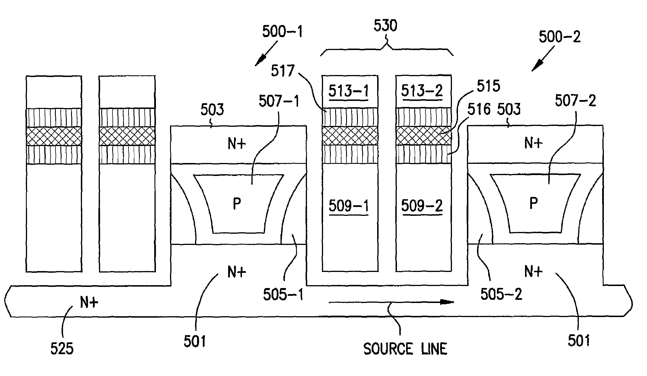
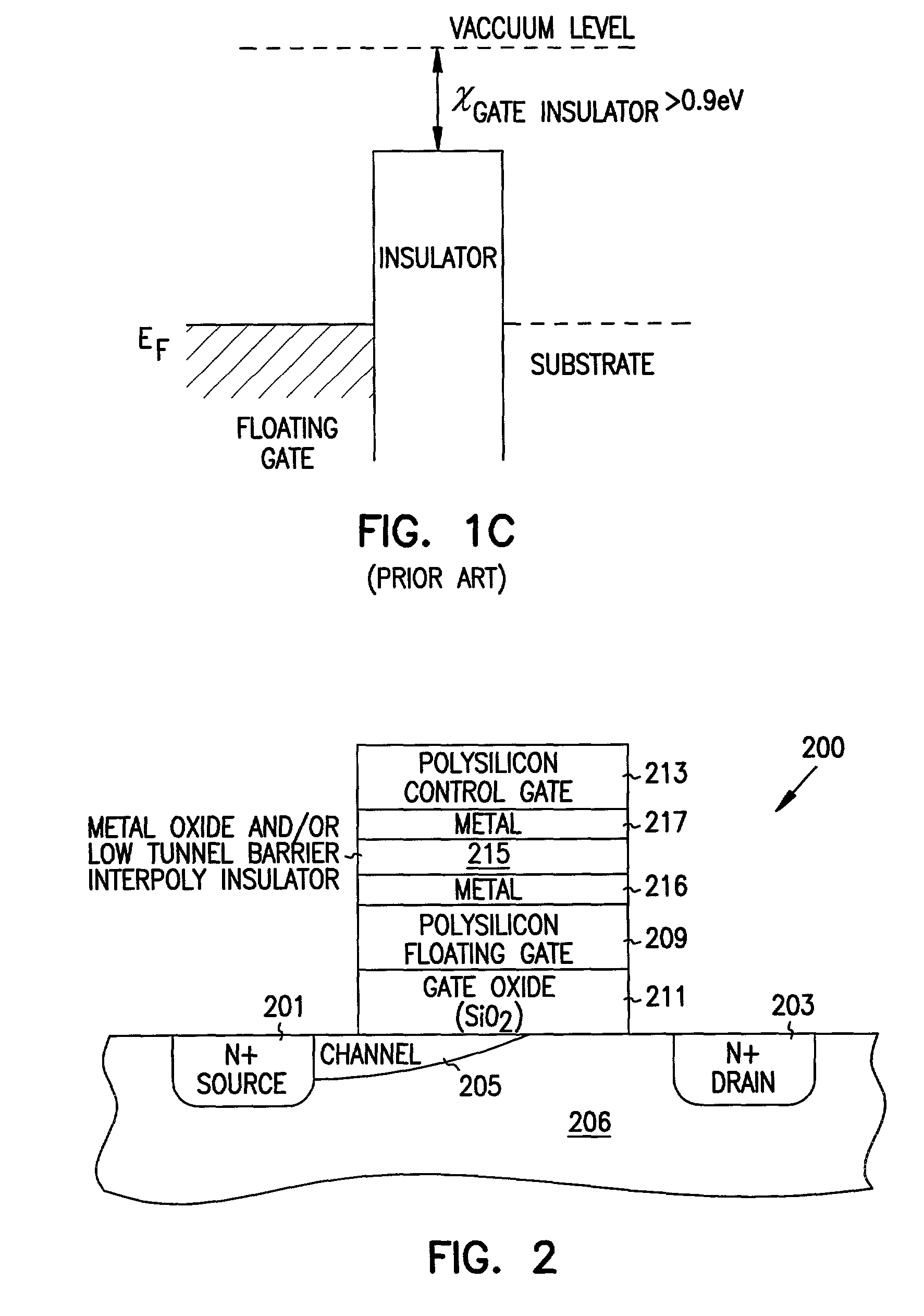
Structures and methods for programmable memory address and decode circuits with low tunnel barrier interpoly insulators are provided. The decoder for a memory device includes a number of address lines and a number of output lines wherein the address lines and the output lines form an array. A number of logic cells are formed at the intersections of output lines and address lines. Each of the logic cells includes a floating gate transistor which includes a first source / drain region and a second source / drain region separated by a channel region in a substrate. A floating gate opposes the channel region and is separated therefrom by a gate oxide. A control gate opposing the floating gate. The control gate is separated from the floating gate by a low tunnel barrier intergate insulator. The low tunnel barrier intergate insulator includes a metal oxide insulator selected from the group consisting of PbO, Al2O3, Ta2O5, TiO2, ZrO2, Nb2O5 and / or a Perovskite oxide tunnel barrier.

Description

CROSS REFERENCE TO RELATED APPLICATIONS[0001]This application is related to the following co-pending, commonly assigned U.S. patent applications: “DRAM Cells with Repressed Memory Metal Oxide Tunnel Insulators,” Ser. No. 09 / 945,395, “Programmable Array Logic or Memory Devices with Asymmetrical Tunnel Barriers,” Ser. No. 09 / 943,134, “Dynamic Electrically Alterable Programmable Memory with Insulating Metal Oxide Interpoly Insulators,” Ser. No. 09 / 945,498, and “Flash Memory with Low Tunnel Barrier Interpoly Insulators,” Ser. No. 09 / 945,507, “SRAM Cells with Repressed Floating Gate Memory, Metal Oxide Tunnel Interpoly Insulators,” Ser. No. 09 / 945,554, which are filed on even date herewith and each of which disclosure is herein incorporated by reference.FIELD OF THE INVENTION[0002]The present invention relates generally to integrated circuits, and in particular to in-service programmable logic arrays with low tunnel barrier interpoly insulators.BACKGROUND OF THE INVENTION[0003]Logic circ...

Claims


Application Information

Patent Timeline
Patent Type & Authority Patents(United States)
IPC IPC(8): G11C16/04H01L21/335H01L21/336H01L21/338H01L29/06G11C8/10G11C16/08
CPCG11C16/08G11C8/10
Inventor FORBES, LEONARD
Owner MICRON TECH INC
Learn More