Deep reactive ion etching process and microelectromechanical devices formed thereby

a deep reactive ion and etching technology, applied in the field of microelectromechanical system (mems) devices formed by etching, can solve the problems of difficult to achieve a 10:1 aspect ratio capable, traditional etching techniques are not generally well suited for mass-producing silicon micromachines, etc., to achieve constant gap width, taper and increase the width of the mask

Inactive Publication Date: 2006-07-18
GOOGLE LLC
View PDF12 Cites 27 Cited by
  • Summary
  • Abstract
  • Description
  • Claims
  • Application Information

AI Technical Summary

Benefits of technology

[0010]The tendency for DRIE to etch wider trenches more rapidly than narrower trenches, a phenomenon which may be termed “etch lag,” is also detrimental to the formation of suspended features for the same reasons explained above. An example is where first and second suspended structures are to be DRIE etched in a substrate over a cavity, in which the first structure is delineated by a wider trench than the second structure. Because the wider trenches of the first structure etch more rapidly during DRIE etching, the wider trenches breach the underlying cavity before the narrower trenches of the second structure, leading to backside erosion and lateral narrowing as explained previously. This phenomenon would be compensated for by masking the substrate so that the masked surface region corresponding to the first structure is intentionally wider than desired, resulting in the adjacent exposed surface regions being narrower than the width desired for the trench that will delineate the first structure, yet wider than the exposed surface regions of the substrate corresponding to the trench that will surround and delineate the second structure. The trench formed in the wider exposed surface regions of the first structure breaches the underlying cavity before the narrower trench of the second structure, with the resulting backside and lateral erosion of the first structure causing the first structure to narrow and eventually substantially acquire its desired width during completion of the etch of the narrower trench surrounding the second structure. However, this scenario is complicated by the findings of the present invention that backside and lateral erosion occur more rapidly with those suspended structures located farther from an anchor site. This invention provides two approaches for addressing this problem. A first is to taper the width of the mask for a suspended structure while maintaining a constant gap width for the exposed surface area in which the trench will be etched to delineate the structure. The mask is tapered to be wider with increasing distance from the anchor site, so that as the width of the mask increases, backside and lateral erosion is correspondingly more rapid to eventually produce a substantially uniform width for the structure. Alternatively, the width of the mask for a suspended structure is maintained constant while tapering the gap width for the exposed surface area in which the trench will be etched to delineate the structure. The gap is tapered to be wider with decreasing distance from the anchor site, so that backside and lateral erosion of the structure that occurs more rapidly with increasing distance from the anchor site is balanced by the more rapid etch rate associated with the increasingly wider gap near the anchor site. As a result, a substantially uniform width for the structure can again be obtained.
[0011]The teachings of this invention concerning the relationship between distance to an anchor site and backside and lateral erosion is also pertinent to other aspects of DRIE etching a MEMS device. As previously noted, a feature of the invention is the ability to properly define specialized elements, such as stiction bumps. According to the invention, stiction bumps must be defined in regions of the substrate away from those areas in which accelerated backside and lateral erosion will occur. Also a feature of this invention is maintaining a proper environment surrounding suspended structures, such as by eliminating unnecessary variations in trench width. An important example is avoiding intersecting trenches that would create a localized wider gap prone to more rapid etching and subsequent backside and lateral erosion, resulting in vertical notches at the intersections.
[0012]In view of the above, it can be seen that the present invention provides a DRIE etching process by which suspended structures of desired widths can be more precisely formed. As a result, the present invention is able to take advantage of the deep etching capability of the DRIE process, while compensating for etch idiosyncrasies that would otherwise adversely affect the structural integrity and durability of a MEMS device, so as to improve yields and device reliability.

Problems solved by technology

However, traditional etching techniques have not generally been well suited for mass-producing silicon micromachines with high aspect ratios necessary to etch closely-spaced fingers in a relatively thick substrate.
For example, with conventional etching techniques it is difficult to achieve a 10:1 aspect ratio capable of forming interdigitized fingers spaced three micrometers apart in a silicon substrate that is thirty micrometers thick.

Method used


Image

  • Deep reactive ion etching process and microelectromechanical devices formed thereby
  • Deep reactive ion etching process and microelectromechanical devices formed thereby
  • Deep reactive ion etching process and microelectromechanical devices formed thereby

Examples


Embodiment Construction

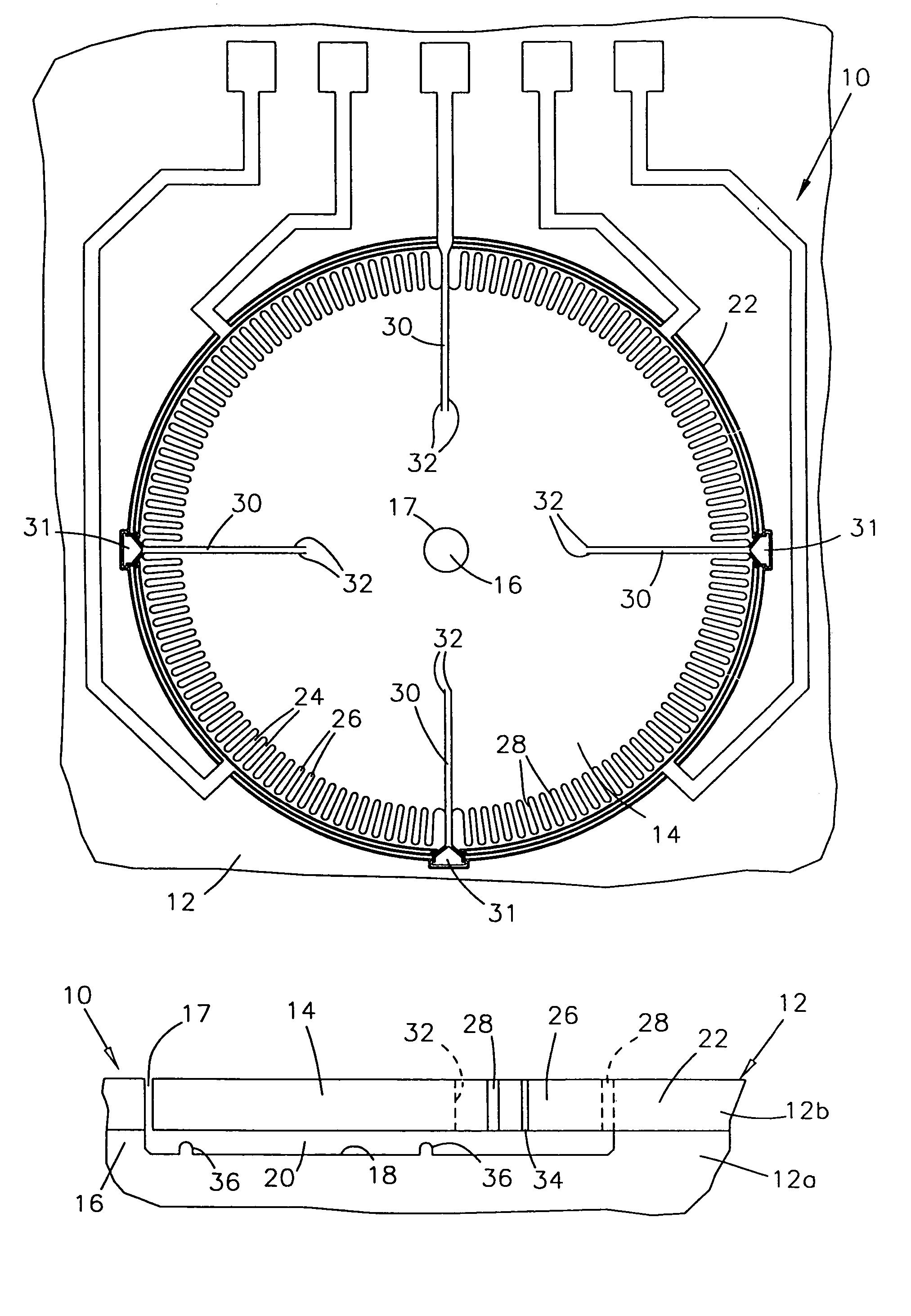
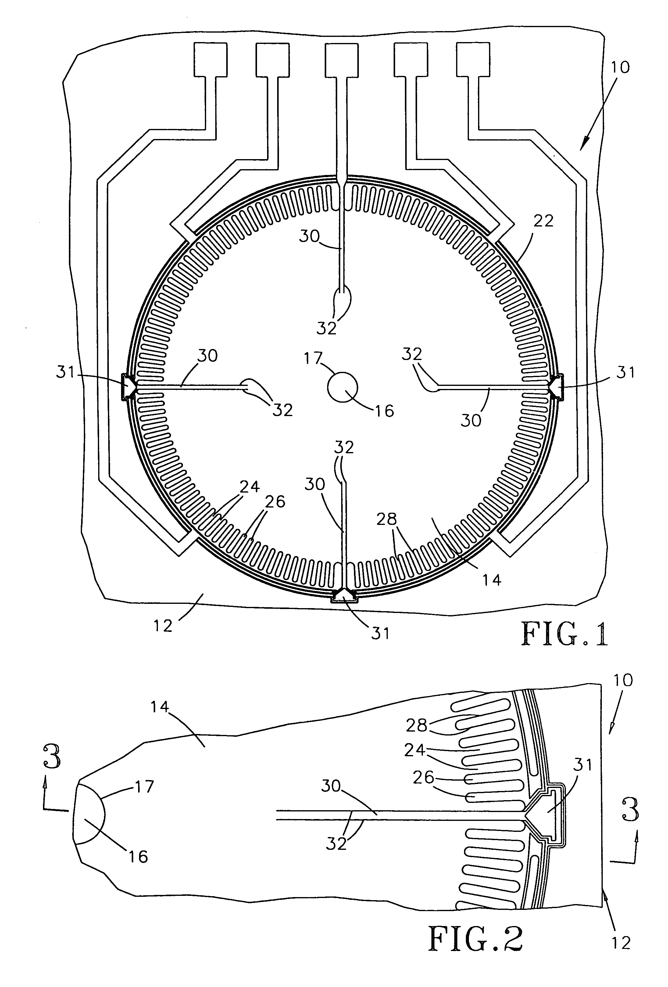
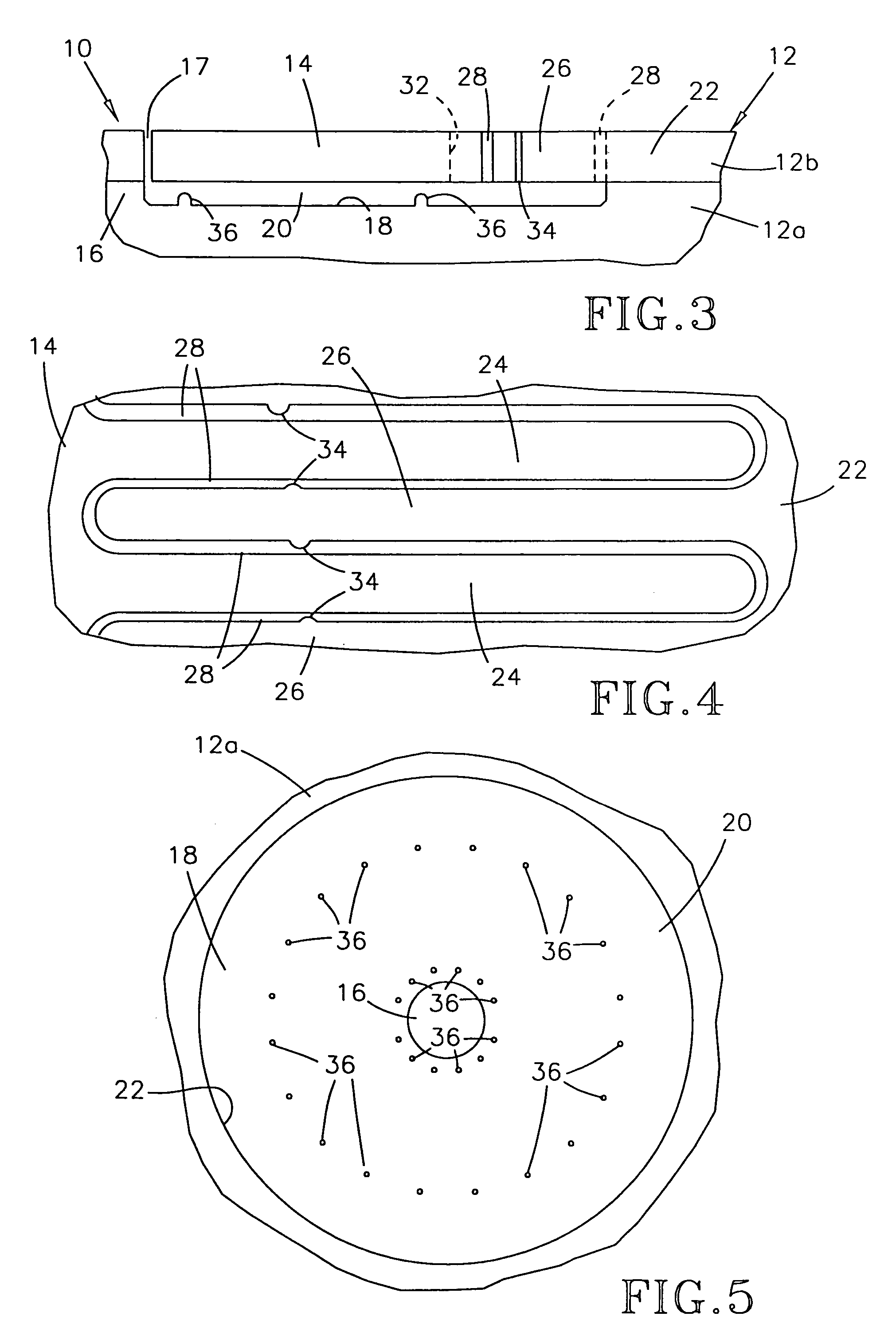
[0021]FIGS. 1 through 5 represent a MEMS device 10 fabricated with a DRIE process in accordance with the present invention, with masking steps of the DRIE process being represented in FIGS. 6 through 8. The device 10 is represented as a rotational accelerometer of the type disclosed by Rich, which is incorporated herein by reference. However, those skilled in the art will appreciate that the device 10 could be employed and modified for a variety of applications, including the rate sensors and accelerometers taught by Putty et al., Sparks and Zarabadi et al.

[0022]As illustrated, the device 10 includes a proof mass 14 formed in a sensing die 12. The die 12 is shown as including a semiconductor layer 12b on a substrate 12a (FIG. 3). A preferred material for the semiconductor layer 12b is epitaxial silicon and a preferred material for the substrate 12a is single-crystal silicon, though it is foreseeable that other materials could be used. For example, the substrate 12b could be formed o...


PUM

PropertyMeasurementUnit
widthaaaaaaaaaa
widthaaaaaaaaaa
widthaaaaaaaaaa

Abstract

A process for forming a microelectromechanical system (MEMS) device by a deep reactive ion etching (DRIE) process during which a substrate overlying a cavity is etched to form trenches that breach the cavity to delineate suspended structures. A first general feature of the process is to define suspended structures with a DRIE process, such that the dimensions desired for the suspended structures are obtained. A second general feature is the proper location of specialized features, such as stiction bumps, vulnerable to erosion caused by the DRIE process. Yet another general feature is to control the environment surrounding suspended structures delineated by DRIE in order to obtain their desired dimensions. A significant problem identified and solved by the invention is the propensity for the DRIE process to etch certain suspended features at different rates. In addition to etching wider trenches more rapidly than narrower trenches, the DRIE process erodes suspended structures more rapidly at greater distances from anchor sites of the substrate being etched. At the masking level, the greater propensity for backside and lateral erosion of certain structures away from substrate anchor sites is exploited so that, at the completion of the etch process, suspended structures have acquired their respective desired widths.

Description

[0001]This is a division of application Ser. No. 09 / 782,393 filed on Feb. 14, 2001, now U.S. Pat. No. 6,685,844.TECHNICAL FIELD[0002]The present invention generally relates to micromachined devices, and particularly microelectromechanical system (MEMS) devices formed by etching processes. More particularly, this invention relates to a micromachining process and design elements for a MEMS device using a deep reactive ion etching (DRIE) process to improve yields and device reliability.BACKGROUND OF THE INVENTION[0003]A wide variety of MEMS devices are known, including accelerometers, rate sensors, actuators, motors, microfluidic mixing devices, springs for optical-moving mirrors, etc. As an example, rotational accelerometers that employ MEMS devices are widely used in computer disk drive read / write heads to compensate for the effects of vibration and shock. Other applications for rotational accelerometers that use MEMS devices include VCR cameras and aerospace and automotive safety co...

Claims


Application Information

Patent Timeline
Patent Type & Authority Patents(United States)
IPC IPC(8): G01P15/00G01P15/125G01P15/14G01P9/00B81C1/00G01P15/08H01L21/00
CPCB81C1/00404G01P15/0802G01P15/0888G01P15/125B81C1/00587H01L21/67069B81C2201/0132B81B2201/025B81B2203/0118
Inventor RICH, DAVID BOYDCHRISTENSON, JOHN C.
Owner GOOGLE LLC
Why Eureka
Try Eureka