

Boride thin films on silicon
a thin film and silicon technology, applied in the field of electronics, can solve the problems of inability to meet the needs of electronic applications, inability to reproduce hts josephson junctions with sufficiently small variations in device parameters, and inability to meet the requirements of electronic applications, etc., to achieve the effect of minimizing magnesium-silicon contaminants, and facilitating the formation of thin films
- Summary
- Abstract
- Description
- Claims
- Application Information
AI Technical Summary
Benefits of technology
Problems solved by technology
Method used
Image

Examples
Embodiment Construction
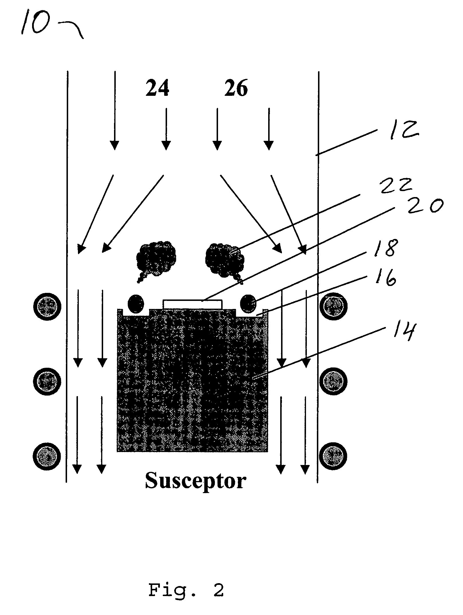
[0019]The present invention contemplates forming thin boron containing films on substrates comprised of silicon by combining, in part, physical vapor deposition (PVD) with chemical vapor deposition (CVD). This hybrid physical chemical vapor deposition (HPCVD) process addresses various problems arising in fabricating thin films of superconducting materials, such as magnesium diboride, which are not readily achieved by either PVD or CVD individually.
[0020]A HPCVD system and its use was described in an earlier Application, U.S. patent application Ser. No. 10 / 395,892 filed 25 Mar. 2003 and entitled “METHOD FOR PRODUCING BORIDE THIN FILMS”, the entire disclosure of which is hereby incorporated by reference herein. This application describes, inter alia, forming magnesium boride films on substrates composed of silicon by HPCVD and discloses the thermodynamics of combining magnesium and boron on a silicon substrate.
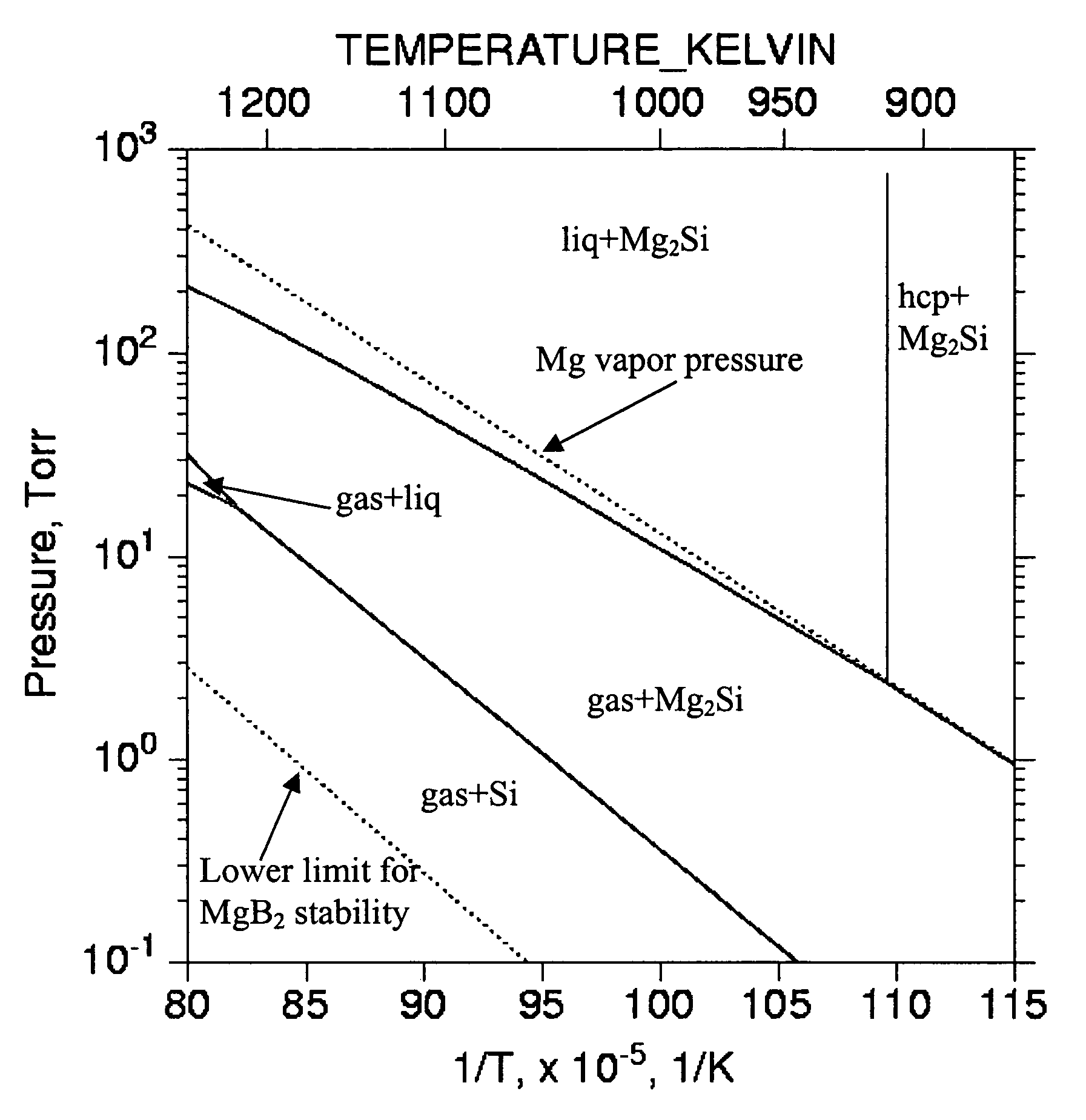
[0021]To better understand the conditions needed for forming thin boride fi...
PUM
| Property | Measurement | Unit |
|---|---|---|
| pressure | aaaaa | aaaaa |
| temperature | aaaaa | aaaaa |
| pressure | aaaaa | aaaaa |
Abstract
Description
Claims
Application Information