Semiconductor device, semiconductor circuit module and manufacturing method of the same

a semiconductor circuit module and semiconductor technology, applied in the direction of semiconductor devices, electrical devices, transistors, etc., can solve the problems of poor crystallinity, inability to obtain a large area, and difficulty in preparing a large diameter substrate by pulling-up method as for the si substrate, so as to reduce the thickness of the single crystal layer and improve the crystallinity. , the effect of good crystallinity

Inactive Publication Date: 2006-08-22
HITACHI LTD
View PDF5 Cites 83 Cited by
  • Summary
  • Abstract
  • Description
  • Claims
  • Application Information

AI Technical Summary

Benefits of technology

[0011]In view of the above, it is an object of the present invention to provide a semiconductor device capable of forming a single crystal layer with good crystallinity comprising Si, Ge, and C on an

Problems solved by technology

Since SiC has a high melting point, it is extremely difficult to prepare a large diameter substrate by the pulling-up method as for the Si substrate.
However, even use of the method still involves a drawback that a substrate having high crystal quality and a large area cannot be obtained.
Further, in a semiconductor integrated circuit for use in communication, not all of the circuits handle signals in a high frequency region since integrated circuits requiring information processing of a large capacity in a low frequency region are also necessary.
The solid solubility of C in Si or SiGe mixed crystal as the diamond structure is several % or less, which involves a drawback that the crystallinity is worsened as the C compositional ratio is increased.
The manufacturing methods r

Method used


Image

  • Semiconductor device, semiconductor circuit module and manufacturing method of the same
  • Semiconductor device, semiconductor circuit module and manufacturing method of the same
  • Semiconductor device, semiconductor circuit module and manufacturing method of the same

Examples


embodiment 1

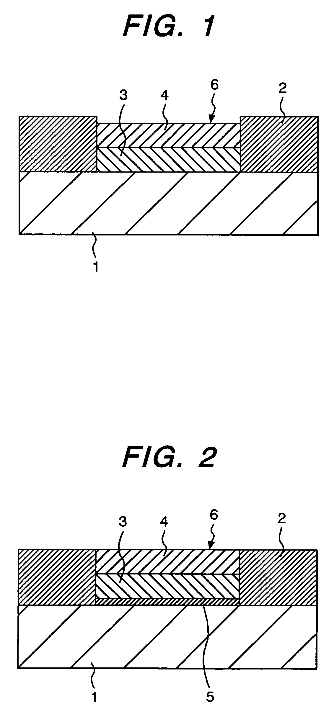
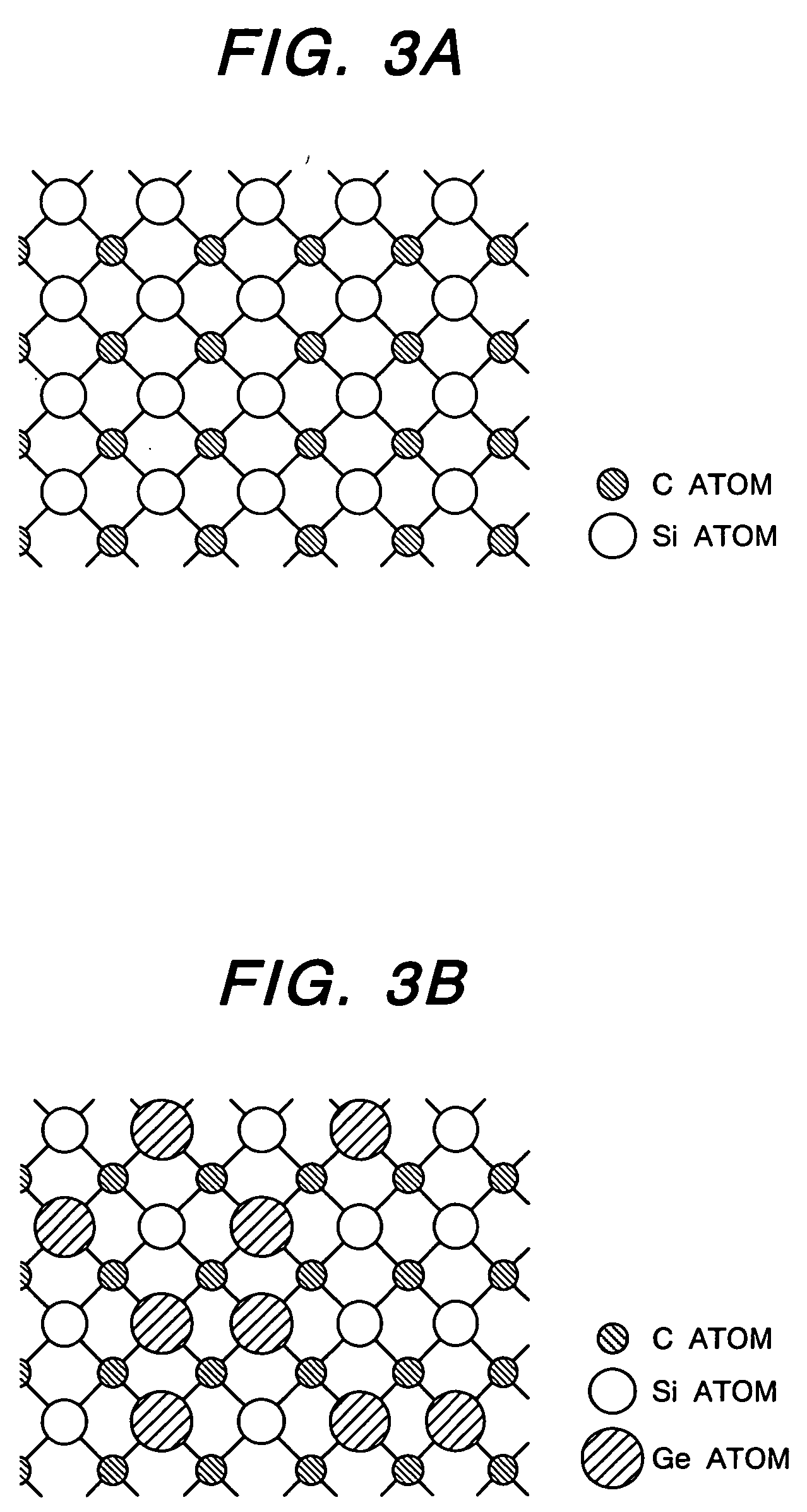
[0067]FIG. 1 is a cross-sectional view showing an embodiment of a semiconductor device according to the present invention. An insulating film 2 having an opening 6 comprising a silicon oxide film is formed on an Si substrate 1. An n-(SiGe)C layer 3 and a p-(SiGe)C layer 4 are formed successively in the opening 6 of the insulating film. In this embodiment, the n-(SiGe)C layer 3 corresponds to the first semiconductor single crystal layer while the p-(SiGe)C layer 4 corresponds to the second semiconductor single crystal layer in the present specification. As described above, the first single crystal layer and the second single crystal layer may each be a single crystal (SiGe)C layer comprising one or both of Si and Ge, and C as essential constitution ingredients, and having a stoichiometric ratio of the sum of Si and Ge to C being substantially 1:1.

[0068]Details of the method of growing the semiconductor single crystal layer according to the invention is to be described with reference ...

embodiment 2

[0106]FIGS. 5A to 5C shows the impurity concentration and the Ge compositional ratio profile, and the band structure of a transistor associated therewith in the intrinsic portion of a bipolar transistor as a second embodiment of a semiconductor device according to the invention. FIG. 5A shows the relationship between the depth from the surface and the impurity concentration, FIG. 5B shows the relationship between the depth from the surface and the Ge compositional ratio, and FIG. 5C shows a band structural view associated therewith. The band structural view shows the upper end a of the valence electron bond and the lower end b of the conduction band. Throughout the drawings 5A to 5C, abscissa shows the depth from the surface in a common manner.

[0107]An n+-Si layer 110 as a high concentration collector region is formed on a silicon substrate, on which an n-SiC layer 111 forming a collector region is formed by epitaxial growing. In this step, as described in Embodiment 1, since a larg...

embodiment 3

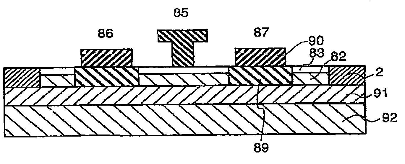
[0120]FIG. 9 shows a cross-sectional structure of a bipolar transistor showing a third embodiment of a semiconductor device according to the invention. This embodiment is characterized by the intrinsic base and an extension structure therefrom.

[0121]A high concentration n-Si layer 52 and a low concentration n-Si layer 53 as a collector are formed on an Si substrate 51. A collector-base insulative layer 54 is formed at the portion other than the active region of the transistor, and a collector extension region 55 is formed in the collector region. A trench 120 is formed by dry etching between the transistors and an insulating film 56 is formed on the inner wall of the trench 120. Then, an insulating film 57 is further buried in the trench 120 to form a device isolation region.

[0122]Collector-base isolation insulating films 58 and 59 are formed and a high concentration collector region 60 is formed. An opening 130 is formed in the collector-base isolation insulating films 59 and 58 to...


PUM


Abstract

An (SiGe)C layer having a stoichiometric ratio of about 1:1 is locally formed on an Si layer, a large forbidden band width semiconductor device is prepared inside the layered structure thereof and an Si semiconductor integrated circuit is formed in the regions not formed with the layered structure, whereby high frequency high power operation of the device is enabled by the large forbidden band width semiconductor device and high performance is attained by hybridization of the Si integrated circuit.

Description

BACKGROUND OF THE INVENTION[0001]The present invention relates to a semiconductor device having a plurality of single crystal semiconductor layers each containing at least one of silicon (Si) and germanium (Ge), and carbon (C) as essential constituent elements and a method of manufacturing the same. The semiconductor device of the invention concerns a technique which is effectively applied to high frequency amplifying semiconductor devices and integrated circuits used in wireless communication apparatus and, further, a technique it is useful for use in broad forbidden band semiconductor devices for wireless communication in quasi-milliwave to milliwave regions.[0002]Along with rapid popularization of mobile communication terminals and internet communication in recent yearn, wireless communication capacity has been increased rapidly year by year. Accordingly, necessary band width in the wireless communication has been extended and increase for the demand of communication apparatus in...

Claims


Application Information

Patent Timeline
IPC IPC(8): H01L29/06H01L31/0328H01L21/331H01L21/04H01L21/338H01L21/8238H01L27/092H01L29/10H01L29/161H01L29/24H01L29/737H01L29/778H01L29/812
CPCH01L21/823807H01L27/0922H01L29/66068H01L29/1054H01L29/1608
Inventor ODA, KATSUYASUGII, NOBUYUKIMIURA, MAKOTOSUZUMURA, ISAOWASHIO, KATSUYOSHI
Owner HITACHI LTD
Why Eureka
Try Eureka