

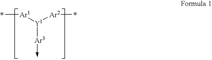
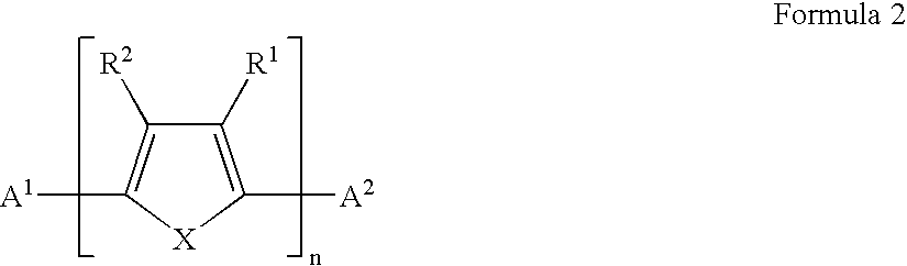
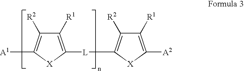
Field effect transistors and materials and methods for their manufacture
a field effect transistor and transistor technology, applied in transistors, solid-state devices, thermoelectric devices, etc., can solve the problems of poor electrical performance, difficult and expensive manufacturing of inorganic materials, and not being completely satisfactory for practical applications
- Summary
- Abstract
- Description
- Claims
- Application Information
AI Technical Summary
Problems solved by technology
Method used
Image

Examples
example 1
Preparation of End Capped 2,4-dimethyl Polymer (Formula 12)
[0072]
This material was prepared using the procedure described in WO 99 / 32537 to yield an off-white solid (20.2 g).(Mw=3100).
example 2
Preparation of 2,4-dimethyl Polymer (Formula 13)
[0073]
Nickel(II) chloride (0.97 g), zinc powder (59.1 g), triphenyl phosphine (39.3 g), 2,2′bipyridyl (1.76 g) and anhydrous N,N-dimethylacetamide (1000 ml) were charged to a 2 litre flask and heated with stirring to 80° C. and a deep red / brown solution was produced—characteristic of formation of the catalyst.
[0074]After 30 minutes at 80° C. the bis(N-4-chlorophenyl)-2,4-dimethylphenylamine (100 g) was added. The oligomerisation was followed by HPLC. After a further 105 minutes the reaction mixture was cooled to room temperature. The reaction mixture was then poured into a 5 litre beaker together with toluene (250 mls). The residual zinc was, then destroyed by slow addition of concentrated hydrochloric acid to the stirred mixture. The organic layer was separated off and washed with water, saturated aqueous sodium bicarbonate solution and finally with water. The organic solution was then dried over magnesium sulfate and filtered. The fi...
example 3
Preparation of Fluorene Polymer (Formula 14)
i) Preparation of 2-bromo-9,9-dimethyl-9H-fluorene
[0082]
[0083]A 1 litre round bottomed flask was charged with 2-bromofluorene (50.0 g), potassium tert-butoxide (68.8 g) and anhydrous dimethyl sulfoxide (DMSO) (210 ml). The reaction mixture immediately became bright red in colour and an exotherm was observed. The reaction mixture was stirred for 30 minutes and then heated on a water bath to 40° C., after which iodomethane (69.5 g, 31 ml) was added dropwise over 3 hours, at a rate such that the temperature did not rise above 45° C. The reaction mixture, now bright purple, was maintained at 45° C. for a further 40 minutes, after which time the reaction was deemed complete. The reaction mixture was allowed to cool to room temperature and poured into a beaker containing distilled water (500 ml) and then extracted with dichloromethane (DCM) (4×300 ml). The aqueous fraction was discarded and the organic solution was washed successively with disti...
PUM
| Property | Measurement | Unit |
|---|---|---|
| molecular weight | aaaaa | aaaaa |
| temperatures | aaaaa | aaaaa |
| molecular weight | aaaaa | aaaaa |
Abstract
Description
Claims
Application Information