Semiconductor laser element

a laser element and semiconductor technology, applied in the direction of laser optical resonator construction, laser details, nanotechnology, etc., can solve the problems of ineffective connection to an optical system, large error in ffp shape calculation, and non-gaussian distribution, so as to achieve high transmittance, suppress light reflection, and improve ffp.

Inactive Publication Date: 2006-09-05
NICHIA CORP
View PDF21 Cites 28 Cited by
  • Summary
  • Abstract
  • Description
  • Claims
  • Application Information

AI Technical Summary

Benefits of technology

[0038]In addition, in the fifth semiconductor laser device of the present invention, both of the first protective membrane and the second protective membrane are formed on the same end. Thereby, it becomes possible to control the light in a transverse direction relative to a main beam.
[0039]In addition, in the fifth semiconductor laser device of the present invention, an emitting plane may be formed so as to be projected. By doing so, release of the light from the vicinity of an emitting part (plane) can be prevented, it becomes possible for the light from the vicinity of the emitting part (plane) to be mixed with the laser light released from an emitting part with difficulty and, thus, better FFP can be easily obtained. In addition, projection of a resonator plane can alter the diverging properties of the laser light.
[0040]In addition, in fifth semiconductor laser device of the present invention, the first protective membrane can be structured by a single-layered or a multi-layered membrane of at least one selected from compounds such as oxides, nitrides and fluorides of Si, Mg, Al, Hf, Nb, Zr, Sc, Ta, Ga, Zn, Y, B and Ti. By using these materials, a protective membrane having the high transmittance can be obtained.
[0041]In addition, in the fifth semiconductor laser device of the present invention, the first protective membrane is a reflection reducing coating (AR membrane (Anti-Reflection Coat)). Thereby, reflection of the light can be suppressed, and the laser light can be effectively emitted.
[0042]In addition, in the fifth semiconductor laser device of the present invention, the first protective membrane having a refractive index which is within ±10% of that of a laminate structure is preferable. Thereby, a device can be protected without altering the properties of the light from an active layer.
[0043]In addition, in the fifth semiconductor laser device of the present invention, it is preferable that the second protective membrane is a shading membrane. This allows the light not to be released to the outside from a part on which the second protective membrane is provided.

Problems solved by technology

However, in such the structure, there is a problem that irregularity (ripple) is generated in far field pattern (FFP), leading to a non-Gaussian distribution.
In a semiconductor laser device in which FFP has a non-Gaussian distribution, there is also a problem that calculation of a shape of FFP makes a great error, and connection to an optical system can not be realized effectively and, for this reason, a driving current becomes great.
In addition, in the previous semiconductor laser device, there is a problem that an emitting end is easily deteriorated.

Method used


Image

  • Semiconductor laser element
  • Semiconductor laser element
  • Semiconductor laser element

Examples


embodiment 3

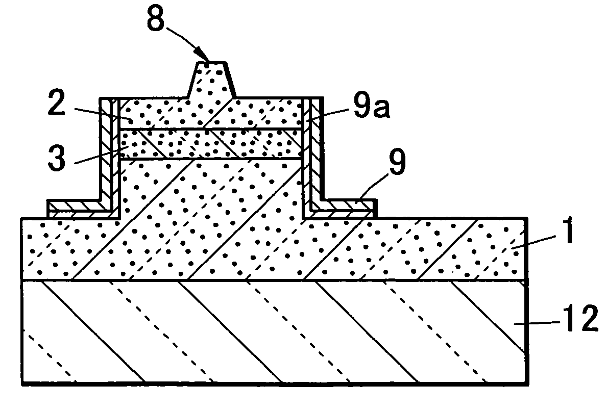
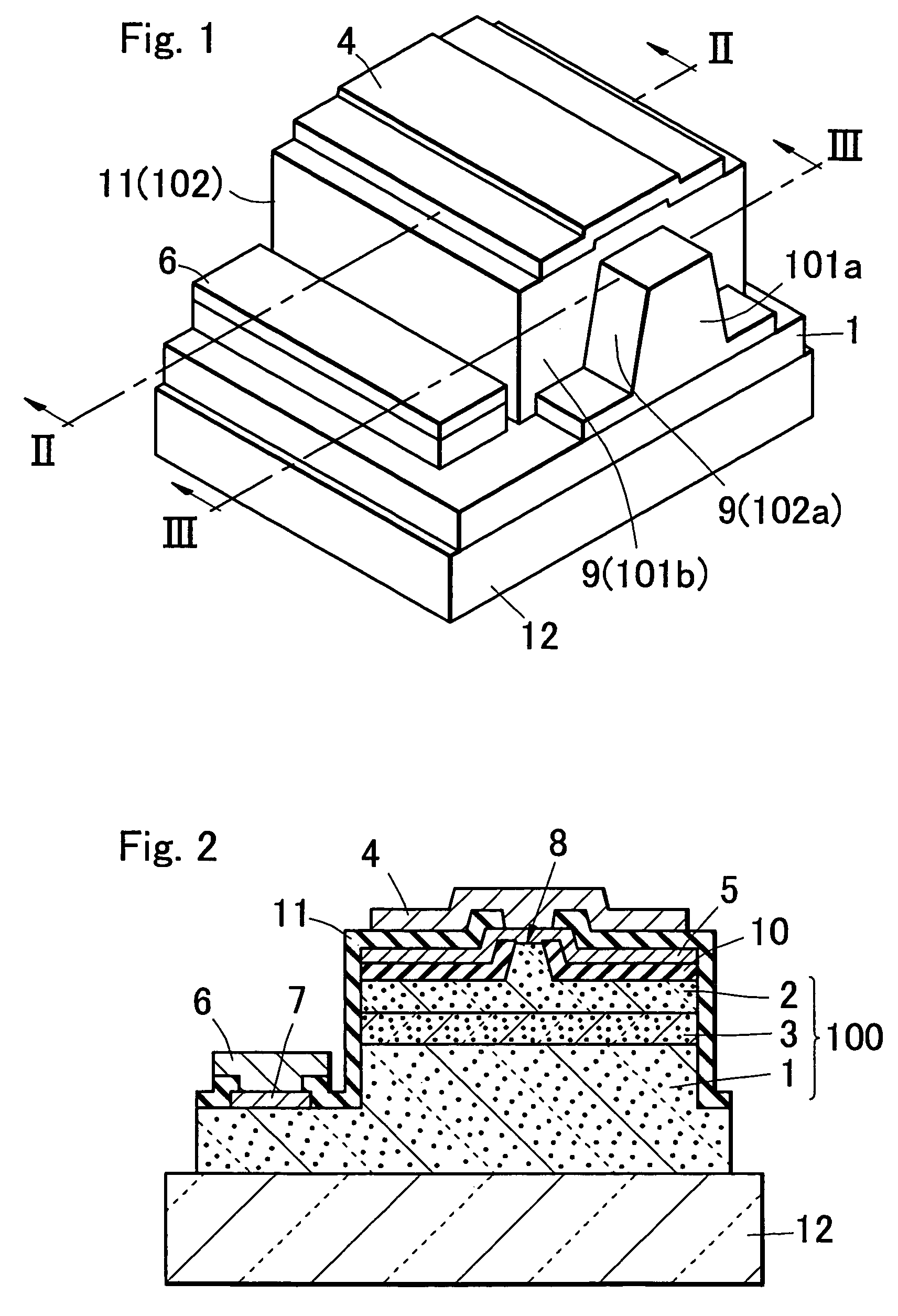
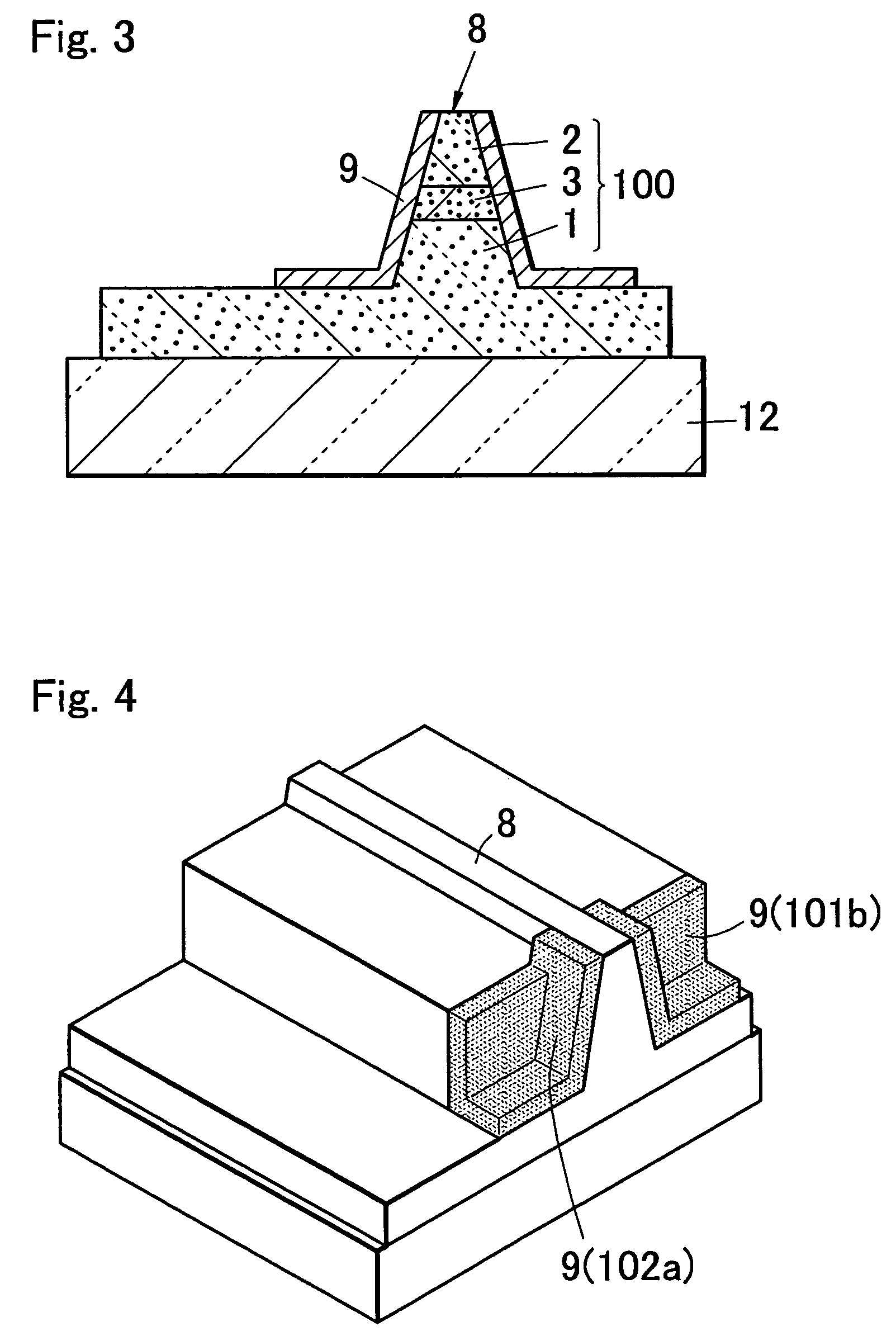
[0136]The semiconductor laser device of an embodiment 3 of the present invention has at least two protective membranes (first protective membrane 109, and a second protective membrane 110 having the lower transmittance than that of the protective membrane 109) having the different light transmittance on an end in a direction vertical to a light resonating direction, and controls release of the light from an end by provision of two protective membranes having the different light transmittance on an end. Specific forms are shown in FIGS. 14A to 14C. In a view of the figure in an embodiment 3, the same parts as those of an embodiment 1 are shown by attaching the same symbols. FIG. 14C is an XIVC—XIVC cross-sectional view of FIG. 14A. In the present embodiment 3, as shown in FIG. 14C, a stripe-like convex part (ridge) 8 is provided in a laminate structure in which a first conductive type semiconductor layer (n-type nitride semiconductor layer) 1, an active layer 3, and a second conducti...

embodiment 4

[0145]As shown in FIG. 17A, FIG. 17B, FIG. 18A and FIG. 18B, the semiconductor laser device of the present embodiment 4 is obtained y applying a first protective membrane 109 and a second protective membrane 110 of an embodiment 3 to a semiconductor laser device having the same end structure as that explained for an embodiment 2, in which both sides of a resonator end are removed below an active layer in the vicinity of a light emitting side resonator plane and a corner part of a laminate structure is removed. That is, in the semiconductor laser device of an embodiment 4, an end in a direction vertical to a light directing direction of a stripe-like waveguide region of a laminate structure is not a single plane, and is composed of a resonator end which is a light emitting plane, and a non-resonator end which is situated on a plane different from the resonator end. In addition, even when seen from a plane (side) parallel with a light directing direction of a stripe-like waveguide reg...

example 1

[0181]In an example 1, a heterogeneous substrate different from a nitride semiconductor is used as a substrate. However, in the present invention, a substrate comprising a nitride semiconductor such as a GaN substrate may be used. Here, as a heterogeneous substrate, for example, substrate materials which can grow a nitride semiconductor can be used, such as sapphire, spinel, ZnS, ZnO, GaAs, Si and SiC having either of C plane, R plane and A plane as a main plane, oxide substrates which are lattice-matched with a nitride semiconductor, and the like. Preferable examples of a heterogeneous substrate include sapphire and spinel. In addition, a heterogeneous substrate may be off angle and, in this case, when step-wisely off angled substrate is used, growth of a ground layer comprising gallium nitride can be performed with the better crystallinity, being preferable. Further, when a heterogeneous substrate is used, a device structure having a single substance substrate of a nitride semicon...


PUM


Abstract

To provide a semiconductor laser device which has no ripple and can afford better FFP having a pattern near a Gaussian distribution upon operation at the high output, the semiconductor laser comprising a laminate structure in which a first conductive type semiconductor layer, an active layer and a second conductive type semiconductor layer different from the first conductive type are laminated in this order, the laminate structure having a waveguide region to guide a light and resonator planes for laser oscillation on both ends, characterized in that the laminate structure has a non-resonator plane on one end side and the non-resonator plane is covered with a shading layer.

Description

TECHNICAL FIELD[0001]The present invention relates to a semiconductor laser device having the better far field pattern (FFP), more particularly, it relates to a semiconductor laser device using a III–V Group nitride semiconductor comprising GaN, AlN or InN, or a mixed crystal thereof (InxAlyGa1-x-yN, 0≦x, 0≦y, x+y≦1).BACKGROUND ART[0002]Recently, a semiconductor laser device has progressed in miniaturization, lightening, high reliance and high output and, thus, is utilized as a light source for personal computers, electronic equipment such as DVD, processing equipment and optical fiber communication. Inter alia, a nitride semiconductor (InxAlyGa1-x-yN, 0≦x, 0≦y, x+y≦1) attracts attention as a semiconductor laser device which can emit from a relatively short wavelength ultraviolet region to a red color.[0003]In such the semiconductor laser device, a buffer layer, an n-type contact layer, a crack-preventing layer, an n-type cladding layer, an n-type light-guiding layer, an active laye...

Claims


Application Information

Patent Timeline
Patent Type & Authority Patents(United States)
IPC IPC(8): H01S5/00H01S5/028H01S5/10H01S5/22H01S5/223H01S5/227H01S5/323H01S5/343
CPCB82Y20/00H01S5/22H01S5/028H01S5/0282H01S5/0286H01S2301/18H01S5/2231H01S5/32341H01S5/34333H01S5/1082
Inventor SUGIMOTO, YASUNOBUOCHIAI, MASANAOYONEDA, AKINORI
Owner NICHIA CORP
Why Eureka
Try Eureka