Method for the assembly of nanowire interconnects

a technology of nanowires and interconnects, which is applied in the direction of nanotechnology, electrical equipment, semiconductor devices, etc., can solve the problems of non-specific binding of wires to targets, the difficulty inherent in handling nanowires, and the functionalization of sensing elements with nanowires, etc., and achieves high aspect ratio, high density, and reduced volume

Active Publication Date: 2006-09-26
UNIV OF SOUTH FLORIDA
View PDF6 Cites 35 Cited by
  • Summary
  • Abstract
  • Description
  • Claims
  • Application Information

AI Technical Summary

Benefits of technology

[0019]Accordingly, the present invention provides a high aspect ratio vertical through-wafer interconnect providing high density systems with reduced volume. In deployment as a sensor, the present invention connects the front side (sensor side) to the back side (package side) through tunable pores filled with metal surrounded by insulator. As such, the silicon dissolution technique in accordance with the present invention is a low cost, high volume manufacturing method when compared to DRIE (Deep Reactive Ion Etching).

Problems solved by technology

In addition to the use of nanowires for packaging, a major impediment in using nanowires for field deployable systems has been the difficulty inherent in handling the nanowires and fun

Method used


Image

  • Method for the assembly of nanowire interconnects
  • Method for the assembly of nanowire interconnects
  • Method for the assembly of nanowire interconnects

Examples


Embodiment Construction

[0031]The longstanding but heretofore unfulfilled need for an improved method for the fabrication of nanowires interconnects is now met by a new, useful, and nonobvious invention.

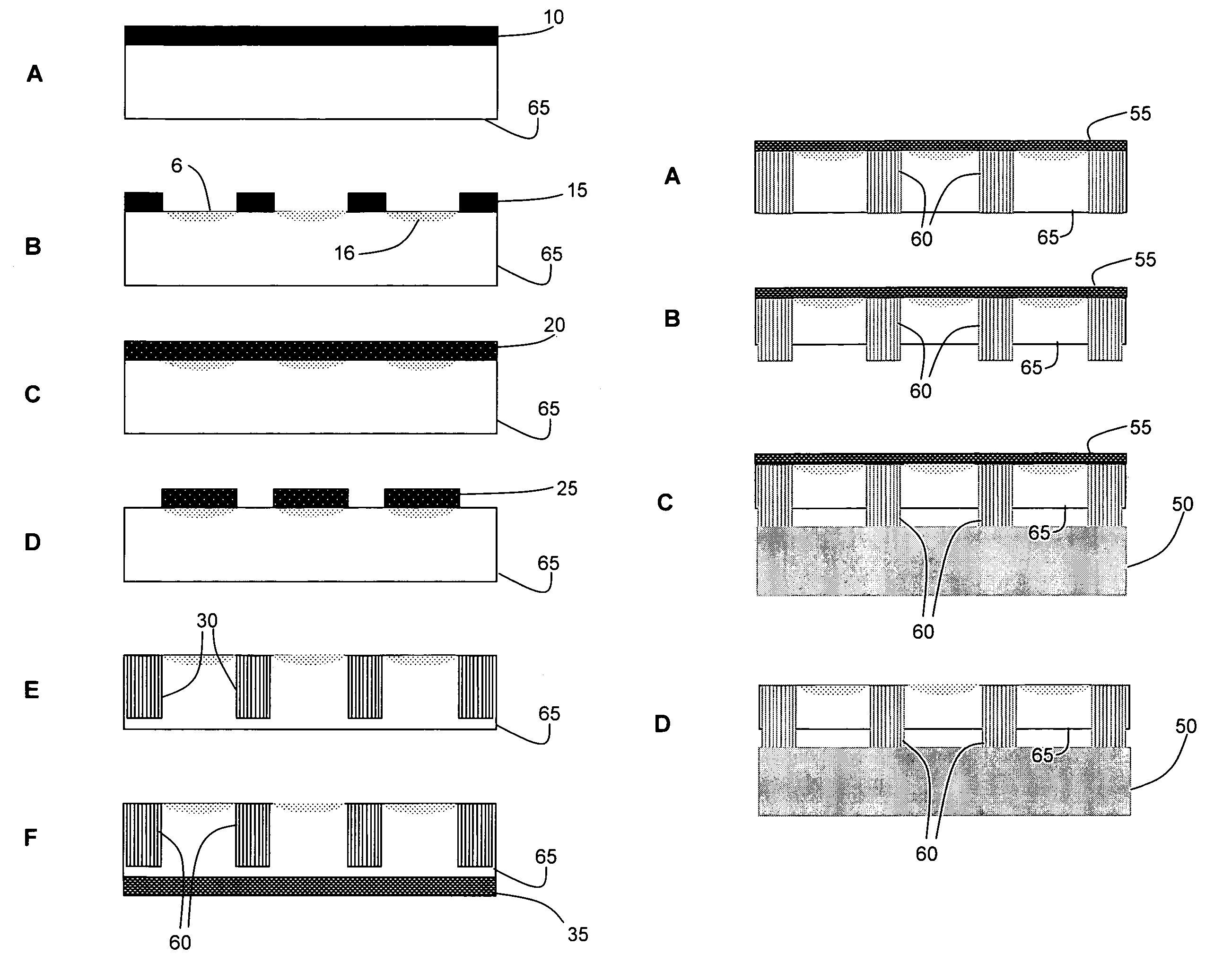
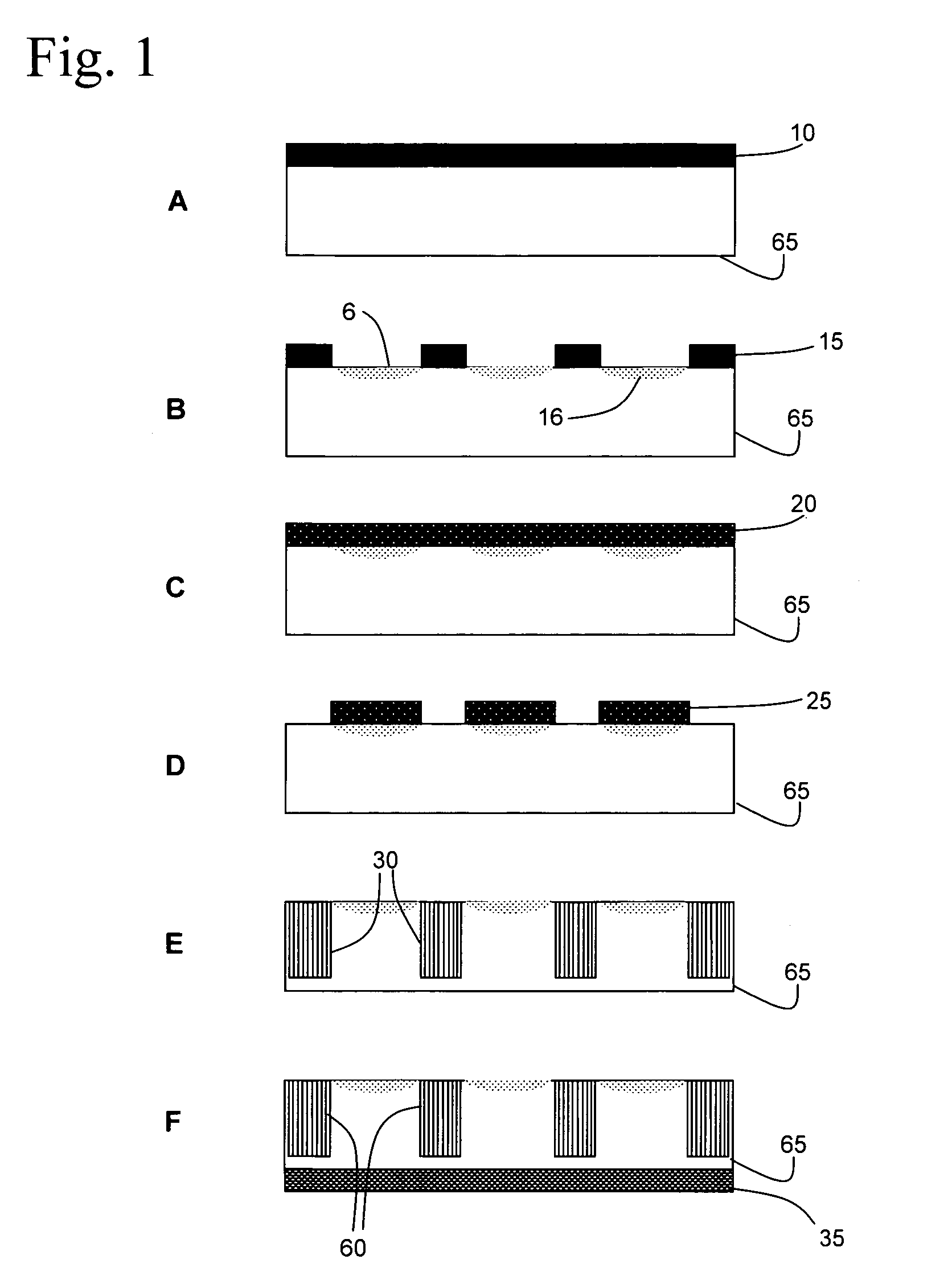
[0032]With reference to FIG. 1, the present invention provides a novel method for synthesizing, functionalizing and attaching nanowires to transductors. In the exemplary embodiment as illustrated in FIG. 1, as shown in FIG. 1A, a silicon template 65 is oxidized 10 and patterned with a desired pattern 15 as shown in FIG. 1B. The silicon template 65 is either p-type or n-type. For a p-type silicon template 65, the surface 6 is then diffused with n-type material 16, following the desired pattern 15. A layer of silicon nitride 20 is then applied 20 as shown in FIG. 1C and patterned 25 to protect the diffused portions of the template as shown in FIG. 1D. The prepared template 65 is then subjected to electrochemical etching to establish pores 30 within the undiffused portions of the template 65 as shown in FIG. 1...


PUM


Abstract

The present invention provides a method for the synthesis of nanowires in a silicon nanoporous template by electrodeposition and a novel technique for the integration of nanowires to transduction surfaces. In accordance with the present invention, a method for the fabrication of nanowire interconnects is provided. The method includes the steps of fabricating substantially vertical nanowires in a selectively passivated nanoporous silicon template, backetching the silicon template to expose the nanowires, eutectically bonding the exposed nanowires to a receiving silicon wafer, and etching the silicon template to produce substantially freestanding nanowire interconnects in contact with the receiving silicon wafer.

Description

CROSS REFERENCE TO RELATED APPLICATION[0001]This application claims priority to U.S. Provisional Patent Application No. 60 / 481,824 entitled: “Nanowire Assembly for Nanoscale Interconnects,” filed by the same inventors on Dec. 22, 2003.BACKGROUND OF INVENTION[0002]Sensors based on metallic nanowires, nanorods and nanoparticles are increasingly being investigated because of unique electronic, optical, biological and magnetic sensing properties that these nanostructures offer. These properties aid in the development of reliable, improved and fast detection techniques for sensors. Templated synthesis of these nanostructures through plating techniques is increasingly being accepted as an elegant alternative to sophisticated methods such as molecular beam epitaxy and e-beam lithography. The advantages of the template method as known in the art are: (a) batch fabrication ability (b) accurate control of the diameter of the pores through controlled pore growth, (c) control of the pore morpho...

Claims


Application Information

Patent Timeline
IPC IPC(8): H01L21/4763
CPCH01L21/76838H01L21/76898Y10S977/721H01L2221/1094
Inventor BHANSALI, SHEKHARARAVAMUDHAN, SHYAMLUONGO, KEVINKEDIA, SUNNY
Owner UNIV OF SOUTH FLORIDA
Why Eureka
Try Eureka