

Semiconductor device including stress inducing films formed over n-channel and p-channel field effect transistors and a method of manufacturing the same
a technology of stress inducing films and semiconductor devices, which is applied in the direction of semiconductor devices, semiconductor/solid-state device details, electrical equipment, etc., can solve problems such as process-induced residual stress in devices
- Summary
- Abstract
- Description
- Claims
- Application Information
AI Technical Summary
Benefits of technology
Problems solved by technology
Method used
Image

Examples
embodiment 1
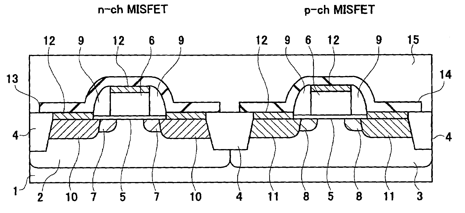
[0060]In the description of Embodiment 1, an example of application of the present invention to a semiconductor device, including a complementary MISFET and having a supply voltage of 1 to 1.5V and a gate length of about 0.1 to 0.14 μm, will be considered.
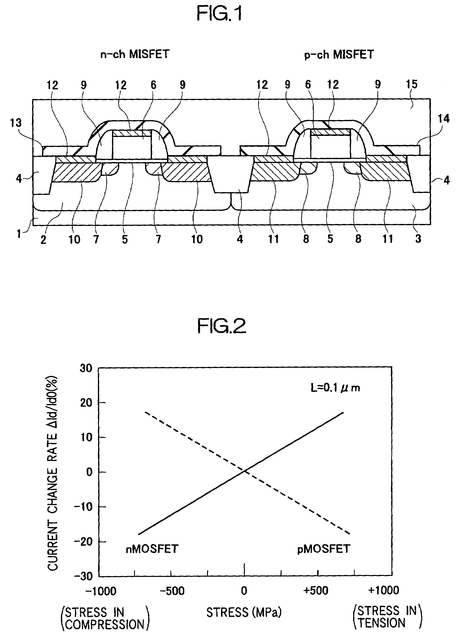
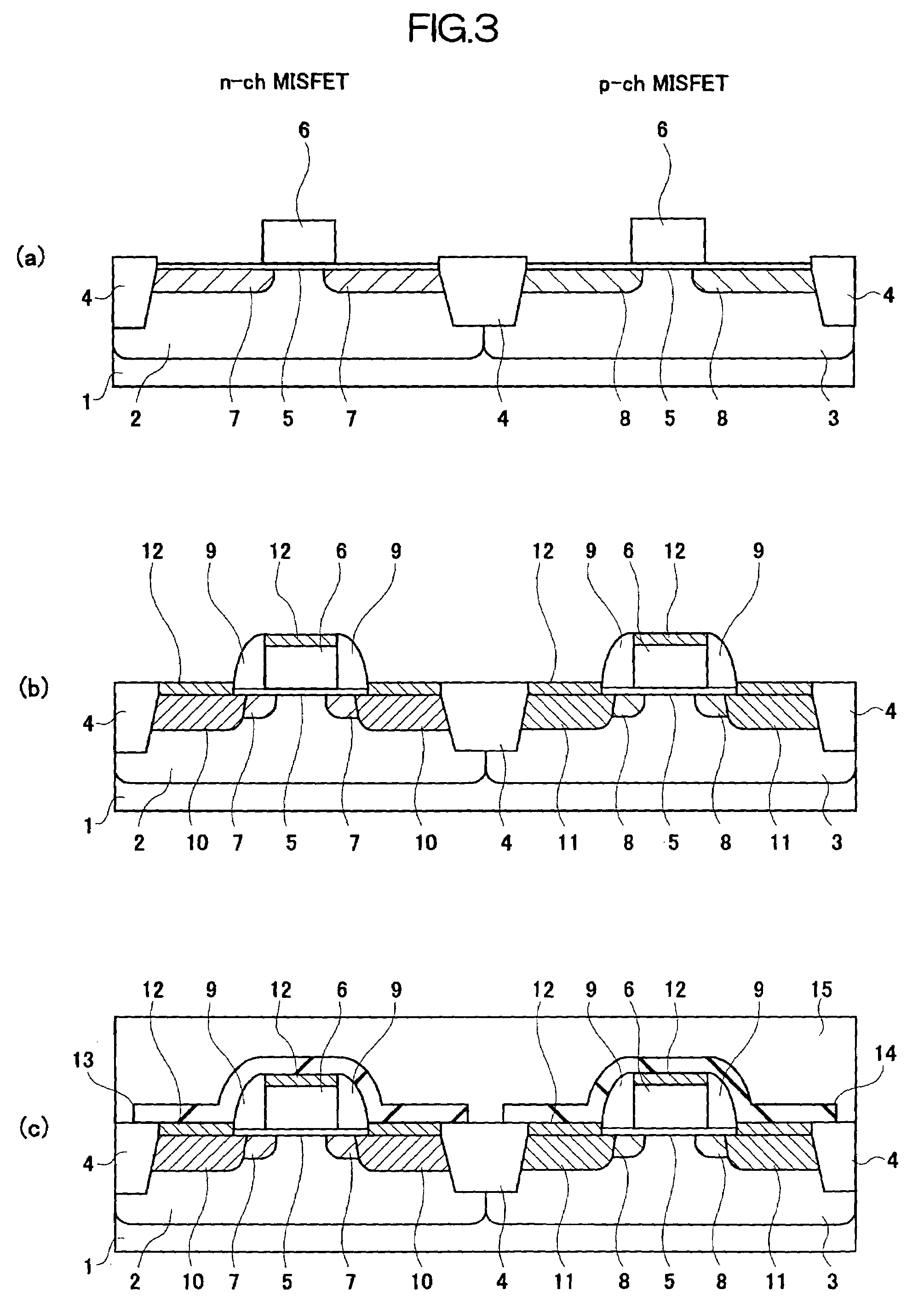
[0061]FIG. 1 is a schematic cross-sectional view roughly illustrating the constitution of a semiconductor device according to Embodiment 1 of the present invention; FIG. 2 is a characteristic diagram illustrating the relation between current driving capacity and film stress; and FIG. 3 is a process flow diagram in which views (a), (b) and (c) are schematic cross-sectional views of the structure in successive steps in the fabrication of the semiconductor device of FIG. 1. In FIG. 1 and FIG. 3, an n channel conductivity type MISFET is illustrated on the left side, while a p channel conductivity type MISFET is illustrated on the right side.
[0062]As illustrated in FIG. 1, the semiconductor device of this Embodiment has, as a semiconduc...
embodiment 2
[0094]This Embodiment 2 has the objective of simplification of the manufacturing steps of the above-described Embodiment 1. FIG. 4 illustrates a process flow in which views (a), (b), (c) and (d) are each a schematic cross-sectional view of the structure in successive steps in the manufacture of a semiconductor device of Embodiment 2 of the present invention.
[0095]As illustrated in FIG. 4 at view (a), n channel conductivity type and p channel conductivity type MISFETs and a silicide layer 12 are formed in a manner similar to Embodiment 1.
[0096]All over the circuit formation surface of the p type substrate 1, a silicon nitride film 13 of about 100 to 120 nm thick is formed as an insulating film by plasma CVD. This silicon nitride film 13 is formed, for example, under conditions of a high frequency power of 350 to 400 W.
[0097]All over the circuit formation surface of the p type substrate 1, a silicon oxide film 13A is formed as an insulating film. This silicon oxide film 13A is, for ex...
embodiment 3
[0103]In the description of Embodiment 3, an example of application of the present invention to a semiconductor device, including a complementary MISFET and having a supply voltage of about 1 to 1.5V and a gate length of 0.1 to 0.14 μm, will be considered.
[0104]This Embodiment 3 has the objective of simplification of the manufacturing steps of the above-described Embodiment 1. FIG. 5 illustrates a process flow in which views (a), (b) and (c) are each a schematic cross-sectional view of the structure in successive steps in the manufacture of a semiconductor device of Embodiment 3 of the present invention. In FIG. 5, an n channel conductivity type MISFET is illustrated on the left side, while a p channel conductivity type MISFET is illustrated on the right side.
[0105]As illustrated in FIG. 5 at view (a), after formation of n channel conductivity type and p channel conductivity type MISFETs and a silicide layer 12 in a manner similar to Embodiment 1, a silicon nitride film 16 for gener...
PUM
 Abstract
Description
Claims
Application Information