

Semiconductor device and method for manufacturing same
- Summary
- Abstract
- Description
- Claims
- Application Information
AI Technical Summary
Benefits of technology
Problems solved by technology
Method used
Image

Examples
example 1
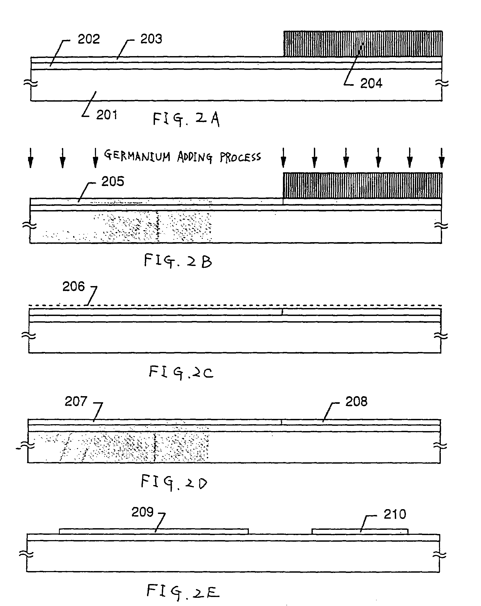
[0039]In this example, an active matrix display device is manufactured as an example having a pixel matrix circuit and a driver circuit (a CMOS circuit is exemplified as a basic unit) formed on an insulating surface of a substrate. This example is explained on a process of forming a substrate with TFTs (referred to as an active matrix substrate), with reference to FIGS. 2A to 2E.
[0040]First, a glass substrate 201 is prepared to form thereon an underlying layer 202 of a silicon oxide film. An amorphous silicon film 203 is formed thereon by a plasma CVD method to a thickness of 30 nm.
[0041]Then a resist mask 204 is provided by patterning on the amorphous silicon film 203. This resist mask 204 is formed in a manner covering the region to be formed with a TFT group for a pixel matrix circuit. That is, an unmasked state is provided for the region to be formed with the circuits, such as a driver circuit and signal processing circuit, requiring high speed characteristics. (FIG. 2A)
[0042]Af...
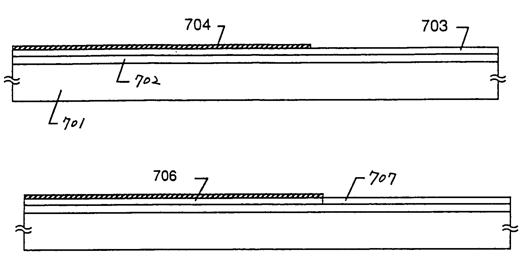
example 2
[0074]In example 1 the catalytic element (nickel) was used to promote crystallization of the amorphous silicon film during its crystallization process. In this example one example is explained on a case of not using nickel with reference to FIGS. 5A and 5B.
[0075]First, a state of FIG. 2B is obtained according to the process of Example 1. Then the resist mask 204 is removed away to carry out a heat treatment at 500° C. for 8 hours. Note that the process temperature is preferably determined in a range of 450 to 600° C. with the process time of 4 to 12 hours.
[0076]In a process of FIG. 5A, crystallization proceeds through the catalytic action of germanium at the region added by germanium, forming a poly silicon germanium region 501. However, natural nucleation can almost neglected for the region not added by germanium. Accordingly, substantial crystallization does not proceed thus forming an amorphous silicon region 502.
[0077]In this manner, the heat treatment condition in this example ...
example 3
[0081]There was shown in Example 2 the case that the heat treatment process was carried out with such a temperature and time that can cause crystallization only at the region added by germanium. In this example, however, explanation is made with reference to FIGS. 6A and 6B for a case where heat treatment is carried out under conditions that can cause crystallization due to natural nucleation also at a region not added by germanium.
[0082]First, a state of FIG. 2B is obtained according to the process of Example 1. Then the resist mask 204 is removed away to carry out a heat treatment at 600° C. for 24 hours. Note that the process temperature is preferably determined in a range of 550 to 650° C. with the process time of 12 to 48 hours.
[0083]In a process of FIG. 6A, crystallization proceeds through the catalytic action of germanium at the region added by germanium, forming a poly silicon germanium region 601. Simultaneously, natural nucleus development occur at the region not added by ...
PUM
 Abstract
Description
Claims
Application Information