Tunnel-junction structure incorporating N-type layer comprising nitrogen and a group VI dopant

a tunnel junction and nitrogen layer technology, applied in semiconductor devices, lasers, semiconductors, etc., can solve the problems of inability to realize the potential of vcsels to generate light with relatively long wavelengths, the use of relativly expensive fabry-perot (fp) and distributed-feedback (dfb) lasers, and the inability to produce reliable, cost-effective vcsels for use at the longer wavelengths used in medium- and long-haul fiber-opti

Active Publication Date: 2006-10-17
AVAGO TECH INT SALES PTE LTD
View PDF11 Cites 39 Cited by
  • Summary
  • Abstract
  • Description
  • Claims
  • Application Information

AI Technical Summary

Benefits of technology

[0025]The voltage drop of the tunnel junction is lowered by forming the tunnel junction structure of a p-type tunnel junction layer and an n-type tunnel junction layer of semiconductor materials selected to have a reduced difference between the valence band energy of the material of the p-type tunnel junction layer and the conduction band energy of the material of the n-type tunnel junction layer. Reducing the energy difference between the valence band energy of the material of the p-type tunnel junction layer and the conduction band energy of the material of the n-type tunnel junction layer increases the tunneling probability at a given reverse bias, and, hence, reduces the voltage drop across the tunnel junction for a given current through the tunnel junction. The difference between the valence band energy of the material of the p-type tunnel junction layer and the conduction band energy of the material of the n-type tunnel junction layer is reduced by adding nitrogen to the gallium arsenide of the n-type tunnel junction layer. The invention eliminates mutual passivation between the nitrogen and the n-type dopant used to dope the material of the n-type tunnel junction layer by doping the material of the n-type tunnel junction layer with a Group VI dopant, such as sulfur (S), selenium (Se), or tellurium (Te). The high active dopant concentration achievable using a group VI dopant further increases the tunneling probability, and reduces the voltage drop across the tunnel junction. In embodiments in which indium (In), antimony (Sb), or bismuth (Bi) is present in the p-type tunnel junction layer, the addition of N to the n-type tunnel junction layer allows the amount of In, Sb, and / or Bi to be increased. This has the effect of increasing the valence band edge in the p-type tunnel junction layer.

Problems solved by technology

Until recently, relatively expensive Fabry-Perot (FP) and distributed-feedback (DFB) lasers have been used to generate light at the wavelengths presently used in the telecommunication industry for transmission via fiber-optic links.
Although VCSEL technology has proven to be a viable lower-cost, lower-power alternative well suited for short-haul network applications, had difficulty to produce reliable, cost-effective VCSELs for use at the longer wavelengths used in medium- and long-haul fiber-optic communications links.
The potential for VCSELs to generate light with relatively long wavelengths has not been realized due, in part, to the difficulty of epitaxially growing DBRs that have suitable optical, electrical, and thermal properties on an indium phosphide (InP) substrate.
Two of the more significant problems are high optical losses and high joule heating in the Bragg mirror fabricated using p-type semiconductor materials.
However, high optical loss in p-type material is a problem.
Such a tunnel junction can therefore be regarded as having a high voltage drop, which is undesirable in many applications.
However, doping concentrations sufficient to ensure a high probability of tunneling are difficult to achieve in these materials.
Unfortunately, when nitrogen is added to the material of the n-type tunnel junction layer, the reduction in the voltage drop across the tunnel junction is less than predicted.

Method used


Image

  • Tunnel-junction structure incorporating N-type layer comprising nitrogen and a group VI dopant
  • Tunnel-junction structure incorporating N-type layer comprising nitrogen and a group VI dopant
  • Tunnel-junction structure incorporating N-type layer comprising nitrogen and a group VI dopant

Examples


Embodiment Construction

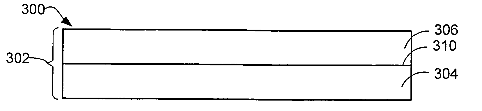
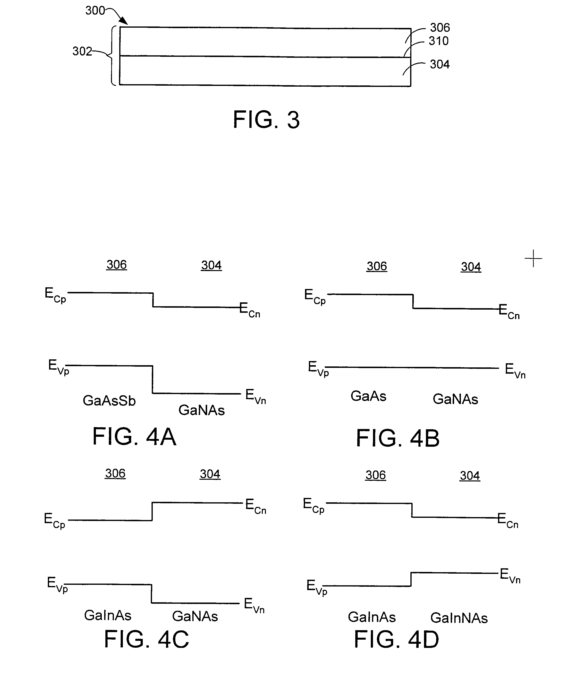
[0038]The invention is based on the realization that the less-than-predicted reduction in the voltage drop across the tunnel junction resulting from adding N to the semiconductor material of the n-type tunnel junction layer is the result of an inadequate concentration of active dopant atoms in the material of the n-type tunnel junction layer. Silicon it typically used as an n-type dopant in Group III–V materials, but a high active dopant concentration is difficult to obtain with this dopant. In a layer of Si-doped GaAs grown by MOCVD, the maximum active dopant concentration practically obtainable is a few times 1018 atoms / cc. This dopant concentration is marginally acceptable in a tunnel junction layer. When nitrogen is added to GaAs as described above, mutual passivation between N and Si reduces the concentration of active dopant atoms. The reduced effective doping concentration gives rise to the less-than-predicted reduction in the voltage drop resulting from adding N to the mater...


PUM


Abstract

A tunnel junction structure comprises an n-type tunnel junction layer of a first semiconductor material, a p-type tunnel junction layer of a second semiconductor material and a tunnel junction between the tunnel junction layers. The first semiconductor material includes gallium (Ga), nitrogen (N), arsenic (As) and is doped with a Group VI dopant. The probability of tunneling is significantly increased, and the voltage drop across the tunnel junction is consequently decreased, by forming the tunnel junction structure of materials having a reduced difference between the valence band energy of the material of the p-type tunnel junction layer and the conduction band energy of the n-type tunnel junction layer. Doping the first semiconductor material n-type with a Group VI dopant maximizes the doping concentration in the first semiconductor material, thus further improving the probability of tunneling.

Description

BACKGROUND OF THE INVENTION[0001]Semiconductor lasers generate light that can be used in optical communication systems, compact disc (CD) players, digital videodisc (DVD) players, scanners and other systems. Semiconductor lasers for optical communications include vertical-cavity surface-emitting lasers (VCSELs), edge-emitting lasers, in-plane emitting lasers and the like.[0002]Until recently, relatively expensive Fabry-Perot (FP) and distributed-feedback (DFB) lasers have been used to generate light at the wavelengths presently used in the telecommunication industry for transmission via fiber-optic links. Although VCSEL technology has proven to be a viable lower-cost, lower-power alternative well suited for short-haul network applications, had difficulty to produce reliable, cost-effective VCSELs for use at the longer wavelengths used in medium- and long-haul fiber-optic communications links.[0003]A VCSEL is composed of an active region sandwiched between vertically-stacked mirrors,...

Claims


Application Information

Patent Timeline
Patent Type & Authority Patents(United States)
IPC IPC(8): H01S3/04H01L29/24H01L31/0336H01S5/00H01S5/024H01S5/042H01S5/183H01S5/22H01S5/30H01S5/343
CPCB82Y20/00H01S5/18308H01S5/305H01S5/024H01S5/0425H01S5/18311H01S5/18369H01S5/3095H01S5/343H01S5/04252H01S5/04254H01S5/02469
Inventor LEARY, MICHAEL HOWARDMARS, DANNY E.ROH, SUNGWON DAVIDCHAMBERLIN, DANIELLE R.CHANG, YING-LAN
Owner AVAGO TECH INT SALES PTE LTD
Why Eureka
Try Eureka