Method and circuit for recovering a data signal from a stream of binary data

a data signal and stream technology, applied in the field of high-speed serial data communication, can solve the problems of reducing the overall performance of multi-channel cr circuits, limiting cr circuit jitter immunity, and further reducing the useful sampling window

Inactive Publication Date: 2006-11-28
IBM CORP
View PDF8 Cites 31 Cited by
  • Summary
  • Abstract
  • Description
  • Claims
  • Application Information

AI Technical Summary

Benefits of technology

[0013]It is another object of the present invention to provide a multichannel receiver that cancels phase errors in the incoming data allowing thereby to deliver in-phase recovered data.
[0014]It is still another object of the present invention to provide an improved method for recovering a digital data signal from a stream of binary data.
[0017]Because the data recovery circuit described above is able to self-detect where the data are to be sampled, it is much less sensitive to jitter (very fast transition detection by construction) and phase errors and thus is well adapted to be placed in a receiver for multichannel long distance high speed serial data communications between integrated circuits / systems. Such a receiver would comprise a plurality of k identical data recovery circuits, one for each data stream and a multiphase clock generator to generate said multiphase clock signal (n phases) that is necessary for its operation. The receiver allows processing of a sampled signal during the totality of one clock period (T) which provides greater margin for error when compared to the time interval between two phases (T / n).

Problems solved by technology

On the other hand, in the case of a multiple channel serial data stream using a single CR circuit, there is an unpredictable phase difference (phase error) between data pertaining to different incoming data streams which limits the CR circuit jitter immunity.
As a matter of fact, both phase error and jitter contribute to the reduction of the overall performance of multichannel CR circuits.
Data jitter and / or phase error between the recovered clock and data signals can further reduce the useful sampling window.
Moreover, circuit manufacturing process deviations, operating temperature and power supply variations can also have a negative impact on the targeted CDR circuit specifications.
It is therefore difficult to ensure that the incoming data signal, which consists of a number of successive bits, is sampled in the centre of the bit time-duration.
First of all, delay elements 13 are noisy and then generate much jitter.
The reference clock needs to be transmitted in addition to the data, thus at the cost of an extra channel.
As a result, circuit 10 is not adapted to long distance multiple channel serial data communications.
Unfortunately, this solution is relatively costly in terms of silicon area and power consumption.
In particular, the filter consumes a large area because it includes high value capacitors (sometimes packaged out of the silicon chip, for instance, mounted on the printed board itself).
Moreover, because it is quite impossible to have a large number of PLL oscillators running at equivalent frequencies, the coupling between PLLs produces interference which are a big concern in terms of jitter.
Finally, it is very unlikely, if not impossible, that the respective recovered clock signals are in phase.
Therefore, implementation of numerous channels (e.g. 16) that are now required for advanced long distance high speed multichannel serial data communications is not satisfactorily achieved to date.

Method used


Image

  • Method and circuit for recovering a data signal from a stream of binary data
  • Method and circuit for recovering a data signal from a stream of binary data
  • Method and circuit for recovering a data signal from a stream of binary data

Examples


Embodiment Construction

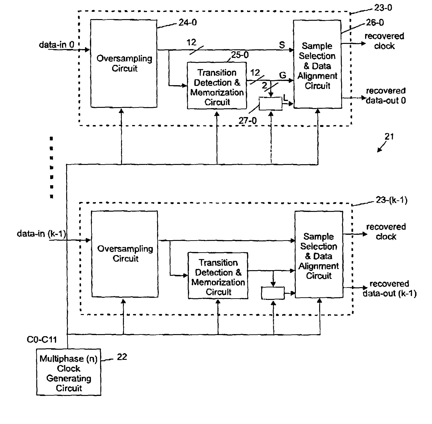
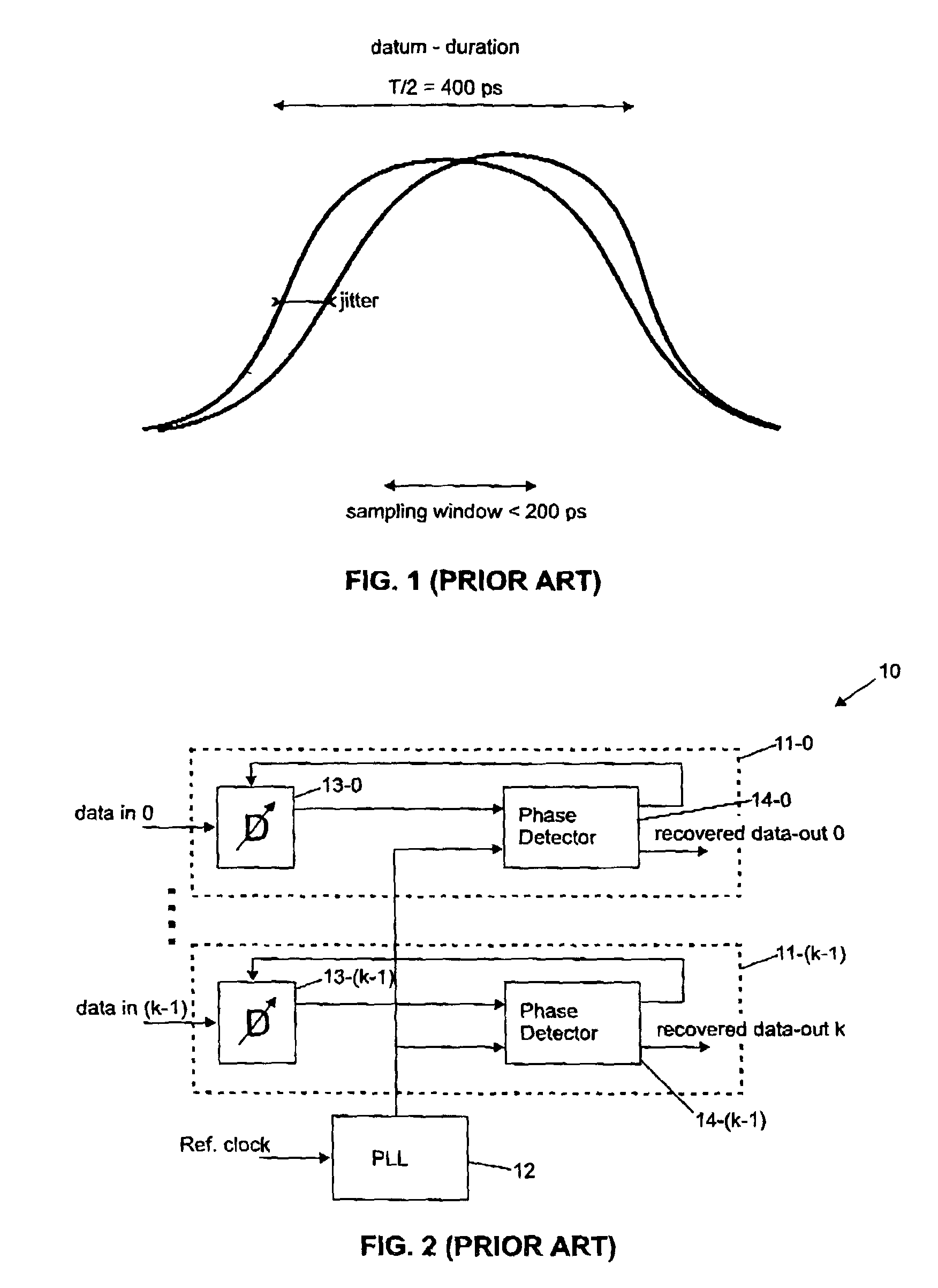
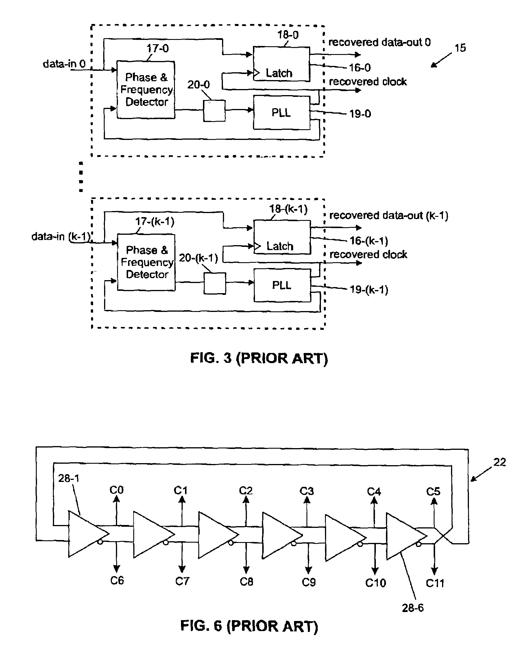
[0034]In the conventional circuits described above by reference to FIGS. 2 and 3, two different phases of a reference clock signal delayed in time are used, one to detect a transition and the other to capture the data for subsequent processing. However, it should be noted that because of possible metastability problems, the particular sampled signal (or sample) obtained by performing the sampling at a data transition (logic state 1 to 0 or vice-versa) is not reliable to accurately locate the exact position of the transition and the detection is even more complicated by the presence of glitches and false detections. As a result, the conventional techniques of sampling that have been practiced so far appear to be close to the limit as the clock frequencies continue to sharply increase.

[0035]In essence, the method of the present invention that will be now described in detail, relies upon an over sampling technique and a specific signal processing method to determine which sampled signa...


PUM


Abstract

There is disclosed a data recovery (DR) circuit including an over sampling (OS) circuit, a transition detection (TD) circuit and a sample selection / data alignment (SSDA) circuit. A multiphase clock generating circuit delivering n phases is coupled to each of these circuits. The OS circuit over samples the received digital data stream and produces n sampled signals at each clock period. The TD circuit is configured to detect a data transition (if any) and to generate n select signals, only one of which is active and represents a determined delay with respect to the transition position, indicating thereby which over sampled signal is the best to be retained. The SSDA circuit is configured to generate the recovered (retimed) data signal that is aligned with a predefined phase of the multiphase clock signal. The data recovery circuit is well adapted to high speed serial data communications between integrated circuits / systems on digital networks.

Description

CROSS REFERENCE TO RELATED APPLICATIONS[0001]Cross reference is hereby made to U.S. patent application Ser. No. 10 / 280,286 entitled “Transition Detection, validation and Memorization Circuit” and Ser. No. 10 / 280,287 entitled “Sample Selection and Data Alignment circuit” which were filed on even date herewith.FIELD OF THE INVENTION [0002]The present invention relates to high speed serial data communications between integrated circuits / systems and more particularly to a data recovery circuit using over sampling which receives a stream of binary data at a determined frequency and supplies a data signal synchronous with a locally generated multiphase clock. The data recovery circuit of the present invention is substantially insensitive to data jitter and phase errors. Therefore, it is well adapted to be incorporated in a receiver to process digital data trains received via different channels from separate sources having no known phase relationship. The present invention also relates to ...

Claims


Application Information

Patent Timeline
Patent Type & Authority Patents(United States)
IPC IPC(8): H04L7/00H04L7/033H04L25/06
CPCH04L7/0338H04L25/068H04L25/069
Inventor VALLET, VINCENTHANVILLER, PHILIPPE
Owner IBM CORP
Why Eureka
Try Eureka