Method for enhancing electrode surface area in DRAM cell capacitors

Inactive Publication Date: 2006-12-12
MICRON TECH INC
View PDF23 Cites 12 Cited by
  • Summary
  • Abstract
  • Description
  • Claims
  • Application Information

AI Technical Summary

Benefits of technology

[0014]Advantageously, the methods of the present invention eliminate the need for random seeding and thermal process conversion as required with respect to an HSG seed layer formation, and provides a greater level of control over topography ordering of the underlayer of a lower capacitor electrode. Unlike prior art methods of forming a capacitor using HSG silicon formation, the texture of the capacitor resulting from the present process is not a randomly created feature, and has a generally uniform pattern and height. Consequently, the size of the capacitor can be more definitively designed and engineered, which facilitates the fabrication of the memory cell. In addition, with

Problems solved by technology

Although the HSG polysilicon increases the surface area of the lower capacitor electrode, current HSG-type methods for increasing capacitor surface area are approaching physical limitations.
A disadvantage of using HSG silicon to form a container type capacitor structure) is that morphology needed to increase surface area is a function of inexact physical conversion of conductive films.
HSG silicon morphology required to gain surface area enhancements needed for next generation part types borders on over-consumed, bulbous grain formations that are structurally unsound.
Current technology does not allow ord

Method used


Image

  • Method for enhancing electrode surface area in DRAM cell capacitors
  • Method for enhancing electrode surface area in DRAM cell capacitors
  • Method for enhancing electrode surface area in DRAM cell capacitors

Examples


Example

[0024]A first embodiment of a method according to the invention is described with reference to FIGS. 2A through 2H, in a method of forming a lower electrode in a capacitor of a DRAM cell.

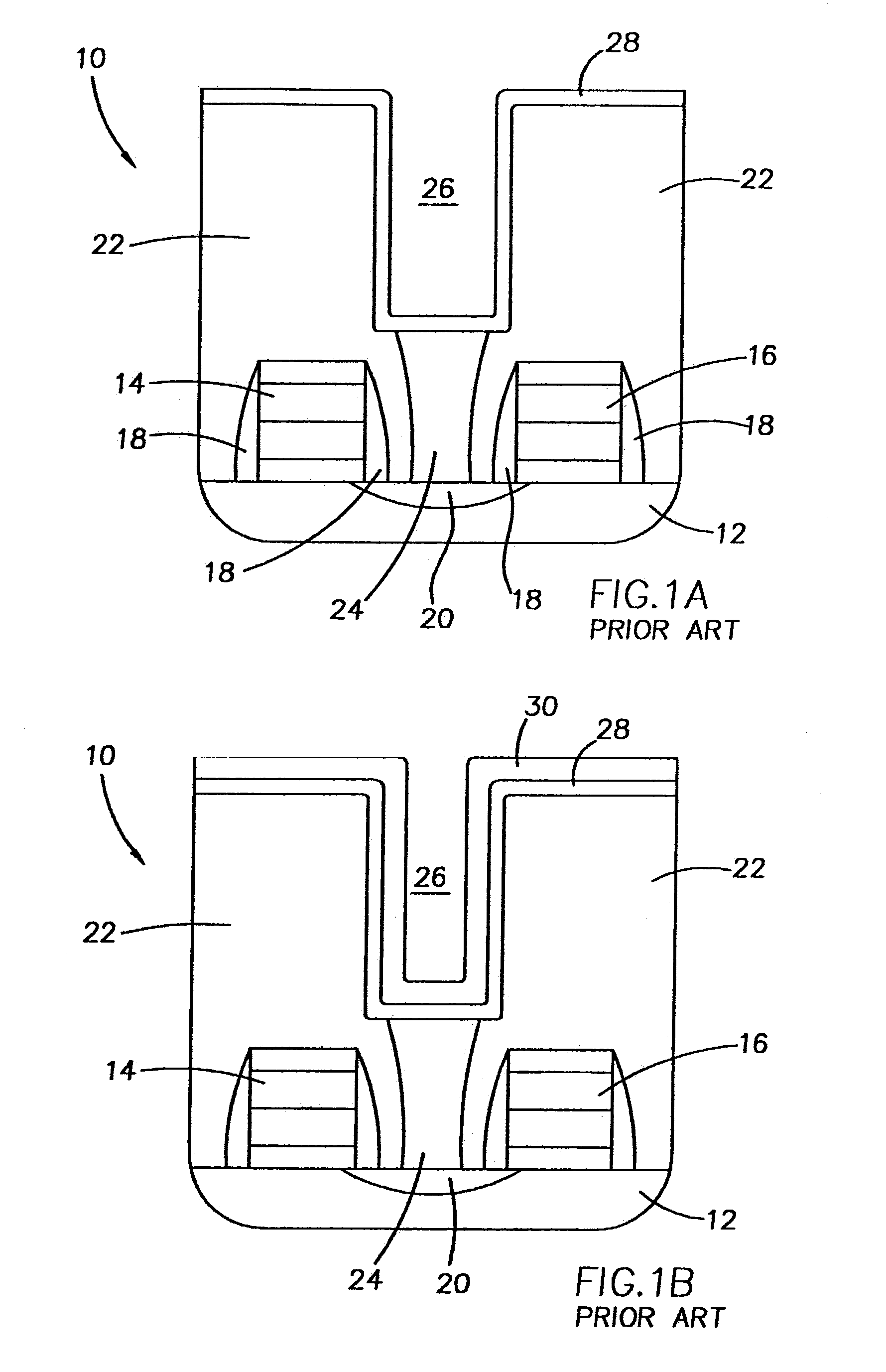
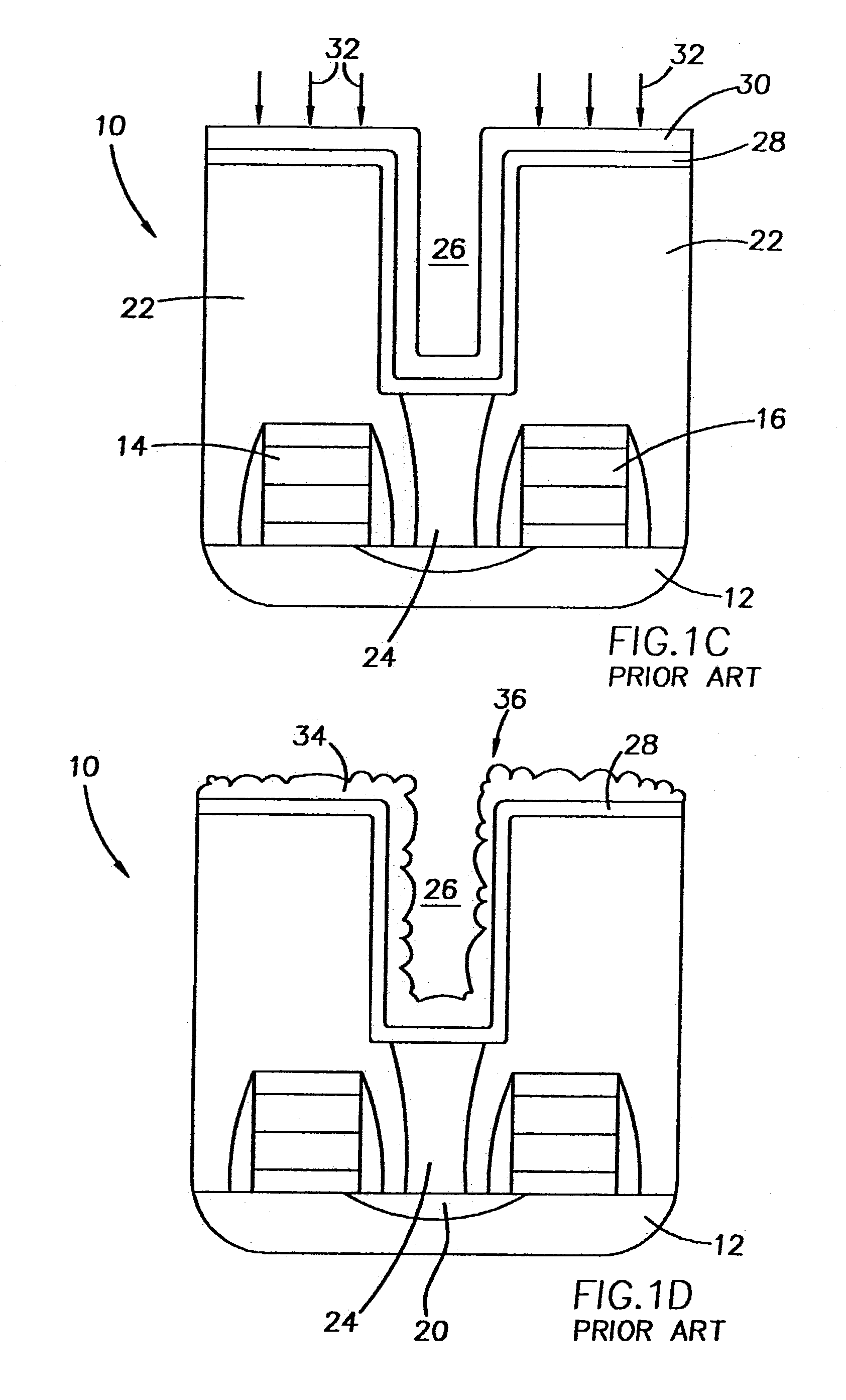
[0025]Referring to FIG. 2A, a wafer fragment 10′ is shown at a preliminary processing step in the formation of a capacitor. The wafer fragment 10′ in progress can comprise a semiconductor wafer substrate or the wafer along with various process layers formed thereon, including one or more semiconductor layers or other formations, and active or operable portions of semiconductor devices.

[0026]The wafer fragment 10′ comprises a substrate 12′ such as monocrystalline silicon, wordlines 14′, 16′, and a diffusion region (active area) 20″ formed in the substrate 12′ between the wordlines, the diffusion region being in the form of a source / drain region. A layer 22′ of BPSG or other suitable insulative material has been deposited over the substrate 12′ and the wordlines 14′, 16′. A plug 24′ comprising doped p...

Example

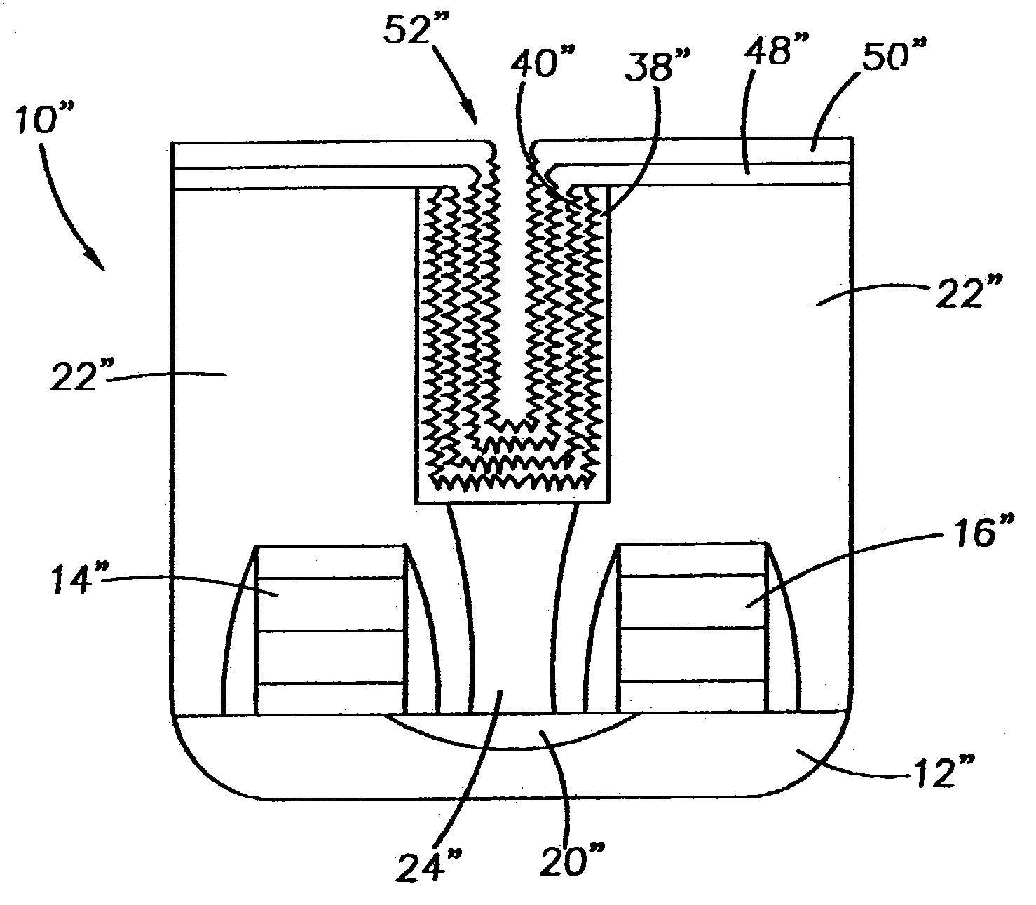
[0045]Referring now to FIGS. 3A through 3F, a second embodiment of a method of the invention is described with reference to forming a lower electrode 42″ in a capacitor 52″. Referring to FIG. 3A, a wafer fragment 10″, similar to the wafer fragment 10′, is shown at a preliminary processing step. The wafer fragment 10″ comprises a substrate 12″, wordlines 14″, 16″, a diffusion region 20″, an insulative layer 22″, plug 24″, and a container 26″.

[0046]Referring to FIG. 3B, a first conductive metal is conformally deposited onto the insulative layer 22″ to form an underlayer 54″, the first conductive metal being platinum (Pt) in the illustrated example. The first conductive metal can be deposited using conventional methods, such as by chemical vapor deposition (CVD), or physical vapor deposition (e.g., sputtering).

[0047]A texturizing layer 38″ is then formed by depositing successive monolayers 56″ of a second conductive metal that is dissimilar to the first conductive metal over the underl...


PUM


Abstract

Methods for forming the lower electrode of a capacitor in a semiconductor circuit, and the capacitors formed by such methods are provided. The lower electrode is fabricated by forming a texturizing underlayer and then depositing a conductive material thereover. In one embodiment of a method of forming the lower electrode, the texturizing layer is formed by depositing a polymeric material comprising a hydrocarbon block and a silicon-containing block, over the insulative layer of a container, and then subsequently converting the polymeric film to relief or porous nanostructures by exposure to UV radiation and ozone, resulting in a textured porous or relief silicon oxycarbide film. A conductive material is then deposited over the texturizing layer resulting in a lower electrode have an upper roughened surface. In another embodiment of a method of forming the lower electrode, the texturizing underlayer is formed by depositing overlying first and second conductive metal layers and annealing the metal layers to form surface dislocations, preferably structured as a periodic network. A conductive metal is then deposited in gaseous phase, and agglomerates onto the surface dislocations of the texturizing layer, forming nanostructures in the form of island clusters. The capacitor is completed by depositing a dielectric layer over the formed lower electrode, and forming an upper capacitor electrode over the dielectric layer. The capacitors are particularly useful in fabricating DRAM cells.

Description

FIELD OF THE INVENTION[0001]The invention relates generally to semiconductor devices, and more particularly to semiconductor capacitor constructions and methods of forming semiconductor capacitors, particularly in applications for forming dynamic random access memory (DRAM) cell structures and integrated circuitry incorporating DRAM cell structures.BACKGROUND OF THE INVENTION[0002]The continuing densification and miniaturization of integrated circuits has led to smaller areas that are available for semiconductor memory devices. For example, in the fabrication of high density dynamic random access memory cells (DRAMs), there is less area available for the storage node (capacitor) of a memory cell. However, the capacitor must have a minimum storage capacitance to ensure operation of the memory cell. There is also a need for increased storage to enable devices to perform more functions at a faster rate.[0003]Several techniques have been developed to increase the storage area of the cap...

Claims


Application Information

Patent Timeline
IPC IPC(8): H01L29/00H01L21/02H01L21/8242H01L27/108
CPCH01L27/1085H01L27/10852H01L28/65H01L28/82H01L28/84H01L28/91H10B12/03H10B12/033B82Y10/00H10B99/00H10B12/00
Inventor YATES, DONALD LMERCALDI, GARRY AHOFMANN, JAMES J
Owner MICRON TECH INC
Why Eureka
Try Eureka