Projection optical system, exposure apparatus, and device production method

Active Publication Date: 2006-12-26
NIKON CORP
View PDF11 Cites 0 Cited by
  • Summary
  • Abstract
  • Description
  • Claims
  • Application Information

AI Technical Summary

Benefits of technology

[0009]As described above, the decrease in the wavelength of exposure light for the improvement in the resolving power poses the problem of the decrease in the transmittance of the optical materials forming the projection optical system and results in limiting types of available optical materials for securing high transmittance. Furthermore, the decrease of transmittance does not cause only loss in quantity of light, but also causes the following disadvantage: part of dissipative light is absorbed by the optical members and the absorbed light turns into heat to cause change in the refractive indices of the optical members or deformation of optical surfaces (lens surfaces), which can result in degrading the imaging performance of the projection optical system.
[0011]The present invention has been accomplished in view of the foregoing problems and an object of the invention is to provide a compact, high-performance projection optical system that decreases the image distortion, while securing a satisfactorily large numerical aperture and a satisfactorily wide imaging area.
[0012]Another object of the present invention is to provide an exposure apparatus that is able to implement excellent projection exposure with a high throughput and a high resolving power, using the compact, high-performance projection optical system. A further object of the present invention is to provide a device production method that can produce an excellent microdevice, using the exposure apparatus capable of implementing excellent projection exposure with a high throughput and a high resolving power.

Problems solved by technology

The various proposals have been made heretofore on the projection optical systems with high resolving power in the prior art, but they failed to secure a sufficiently wide, effective exposure area (image field: imaging area).
As described above, the decrease in the wavelength of exposure light for the improvement in the resolving power poses the problem of the decrease in the transmittance of the optical materials forming the projection optical system and results in limiting types of available optical materials for securing high transmittance.
Furthermore, the decrease of transmittance does not cause only loss in quantity of light, but also causes the following disadvantage: part of dissipative light is absorbed by the optical members and the absorbed light turns into heat to cause change in the refractive indices of the optical members or deformation of optical surfaces (lens surfaces), which can result in degrading the imaging performance of the projection optical system.
Correction for aberration is necessary for the widening of the field and the increase of the resolving power, but it is extremely difficult to make correction for aberration throughout the whole of the wide exposure area with use of the limited types of optical materials.

Method used


Image

  • Projection optical system, exposure apparatus, and device production method
  • Projection optical system, exposure apparatus, and device production method
  • Projection optical system, exposure apparatus, and device production method

Examples


first embodiment

[First Embodiment]

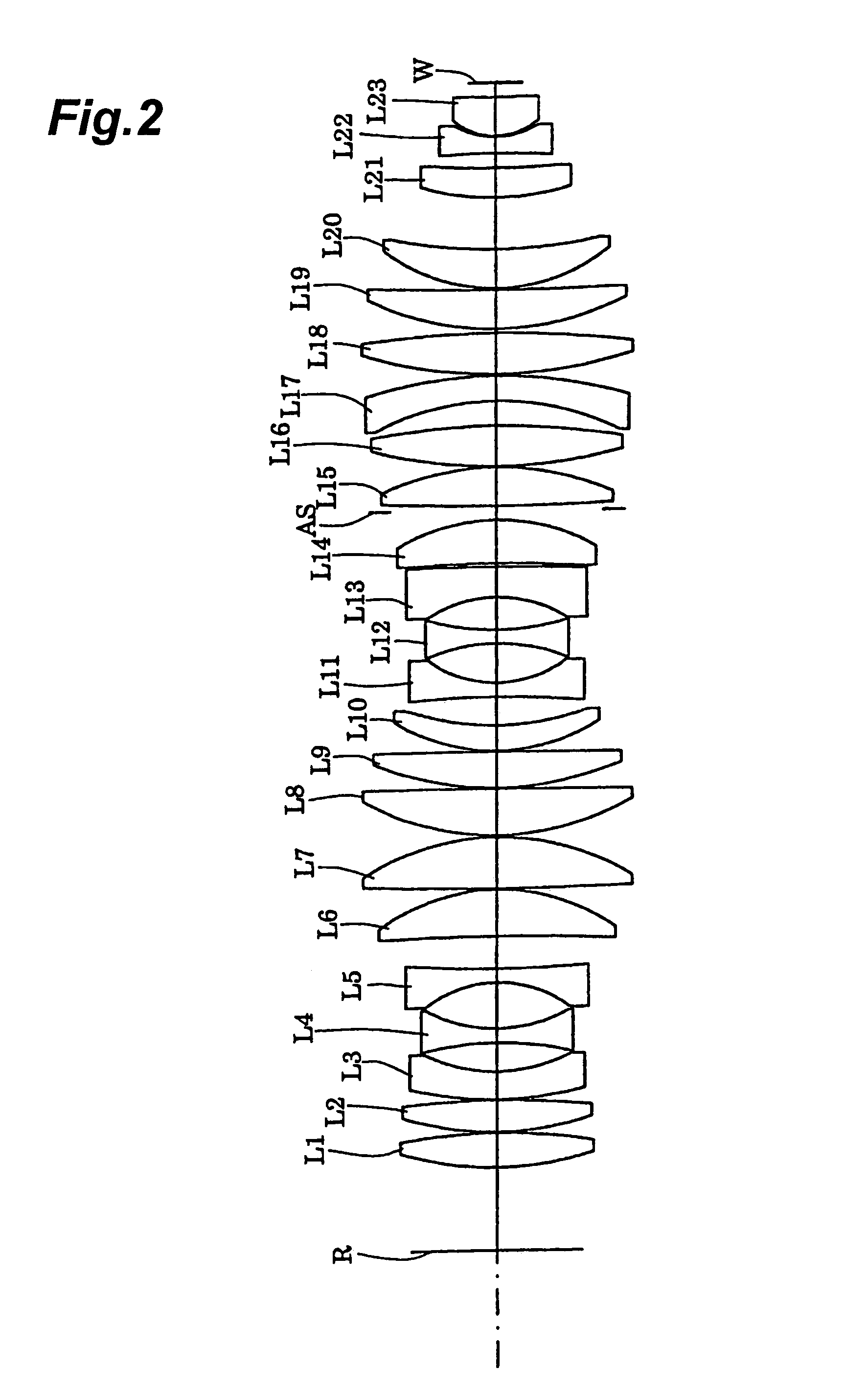
[0072]FIG. 2 is a drawing showing the lens setup of the projection optical system according to the first embodiment. With reference to FIG. 2, the projection optical system PL of the first embodiment is comprised of the following lenses named in order from the reticle side: biconvex lens L1, biconvex lens L2, negative meniscus lens L3 with a concave surface of aspherical shape facing the wafer side, biconcave lens L4, biconcave lens L5, positive meniscus lens L6 with a concave surface facing the reticle side, biconvex lens L7, plano-convex lens L8 with the plane facing the wafer side, plano-convex lens L9 with the plane facing the wafer side, positive meniscus lens L10 with a concave surface of aspherical shape facing the wafer side, biconcave lens L11, biconcave lens L12 with a concave surface of aspherical shape facing the wafer side, negative meniscus lens L13 with a concave surface facing the reticle side, positive meniscus lens L14 with a concave surface facin...

second embodiment

[Second Embodiment]

[0078]FIG. 5 is a drawing showing the lens setup of the projection optical system according to the second embodiment. With reference to FIG. 5, the projection optical system PL of the second embodiment is comprised of the following lenses named in order from the reticle side: biconvex lens L1, biconvex lens L2, negative meniscus lens L3 with a concave surface of aspherical shape facing the wafer side, biconcave lens L4, biconcave lens L5 with a concave surface of aspherical shape facing the wafer side, negative meniscus lens L6 with a concave surface facing the reticle side, positive meniscus lens L7 with a concave surface facing the reticle side, positive meniscus lens L8 with a concave surface facing the reticle side, biconvex lens L9, positive meniscus lens L10 with a convex surface facing the reticle side, biconcave lens L11 with a concave surface of aspherical shape facing the wafer side, biconcave lens L12 with a concave surface of aspherical shape facing th...

third embodiment

[Third Embodiment]

[0084]FIG. 8 is a drawing showing the lens setup of the projection optical system according to the third embodiment. With reference to FIG. 8, the projection optical system PL of the third embodiment is comprised of the following lenses named in order from the reticle side: negative meniscus lens L1 with a convex surface facing the reticle side, a biconcave lens L2 with a concave surface of aspherical shape facing the reticle side, positive meniscus lens L3 with a concave surface facing the reticle side, positive meniscus lens L4 with a concave surface facing the reticle side, positive meniscus lens L5 with a convex surface facing the reticle side, biconvex lens L6, biconvex lens L7, negative meniscus lens L8 with a concave surface of aspherical shape facing the wafer side, negative meniscus lens L9 with a concave surface of aspherical shape facing the wafer side, biconcave lens L10 with a concave surface of aspherical shape facing the wafer side, biconcave lens L1...


PUM


Abstract

Provided is a projection optical system for forming an image of a pattern of a first object (R) on a second object (W). The projection optical system is made of an optical material having a refractive index of not more than 1.6 and is substantially telecentric both on the first object side and on the second object side. The projection optical system satisfies the condition of (λ×L) / (NA×Y02)<1.5×10⁻³, where λ is a wavelength of light, L a distance between the first object and the second object, MA a numerical aperture on the second object side, and Y0 a maximum image height on the second object.

Description

BACKGROUND OF THE INVENTION[0001]1. Field of the Invention[0002]The present invention relates to a projection optical system, an exposure apparatus, and a device production method and, more particularly, to a projection optical system suitably applicable to exposure apparatus used in production of microdevices such as semiconductor devices and liquid crystal display devices by photolithography.[0003]2. Related Background Art[0004]For producing the semiconductor devices and others, the exposure apparatus is used for transferring an image of a pattern on a reticle as a mask through the projection optical system onto a wafer (or a glass plate or the like) coated with a photoresist. Concerning the exposure apparatus of this type, there are increasing demands for improvement in the resolving power of the projection optical system, with progress in miniaturization of patterns of semiconductor integrated circuits or the like. A potential way for the improvement in the resolving power of th...

Claims


Application Information

Patent Timeline
IPC IPC(8): G03B27/54G02B9/00G02B13/24G02B13/14G02B13/18G02B13/22G03F7/20H01L21/027
CPCG02B13/146G03F7/703G03F7/70241H01L21/027
Inventor SHIGEMATSU, KOJIFUJISHIMA, YOUHEIOMURA, YASUHIROISHIYAMA, TOSHIRO
Owner NIKON CORP
Why Eureka
Try Eureka