Optically active substrates

a substrate and optically active technology, applied in the field of optical scanning or imaging, can solve the problems of high initial cost, relatively inefficient process of fluorescence microscopy, time and cost of associated labor, etc., and achieve the effect of high index of refraction

Inactive Publication Date: 2007-01-02
AFFYMETRIX INC
View PDF99 Cites 43 Cited by
  • Summary
  • Abstract
  • Description
  • Claims
  • Application Information

AI Technical Summary

Benefits of technology

[0019]The optically transparent substrate has a thickness between the first and second surface of about 1 mm. Each said micro-optical element has a dimension comparable to, or somewhat larger or smaller than the wavelength of the radiation. The surface of the micro-optical elements may include a layer of a high index medium transparent at the employed wavelengths. The high index medium is deposited by one of the following: sputtering, evaporation, or MOCVD.
[0020]The micro-optical elements may include high density micro-lenses having a high index of refraction. The high density micro-lenses with the high index of refraction are made by vacuum deposition onto the first surface.
[0021]The micro-optical elements may be micro-lenses or other elements formed inside or on the surface of the substrate, having a radius or other periodic dimension in the range of 0.1 μm to 10 μm, or for some structures less than 100 μm. Preferably, the dimensions are comparable to the wavelength.

Problems solved by technology

Although the initial cost may be high, overall the technology represents considerable savings in the time and costs of associated labor.
Fluorescence microscopy is a relatively inefficient process, wherein the light source-to-detector efficiency is estimated in parts per trillions.
There is usually a very low efficiency of the fluorescence conversion.
Furthermore, among other limitations, the scanning systems cannot increase the intensity of the illumination by the laser source, because the fluorescent sample would be destroyed; this is known as photo-bleaching.
Also, before photo-bleaching takes place, most fluorophores behave in a non-linear and possibly unpredictable manner.

Method used


Image

  • Optically active substrates
  • Optically active substrates
  • Optically active substrates

Examples


Embodiment Construction

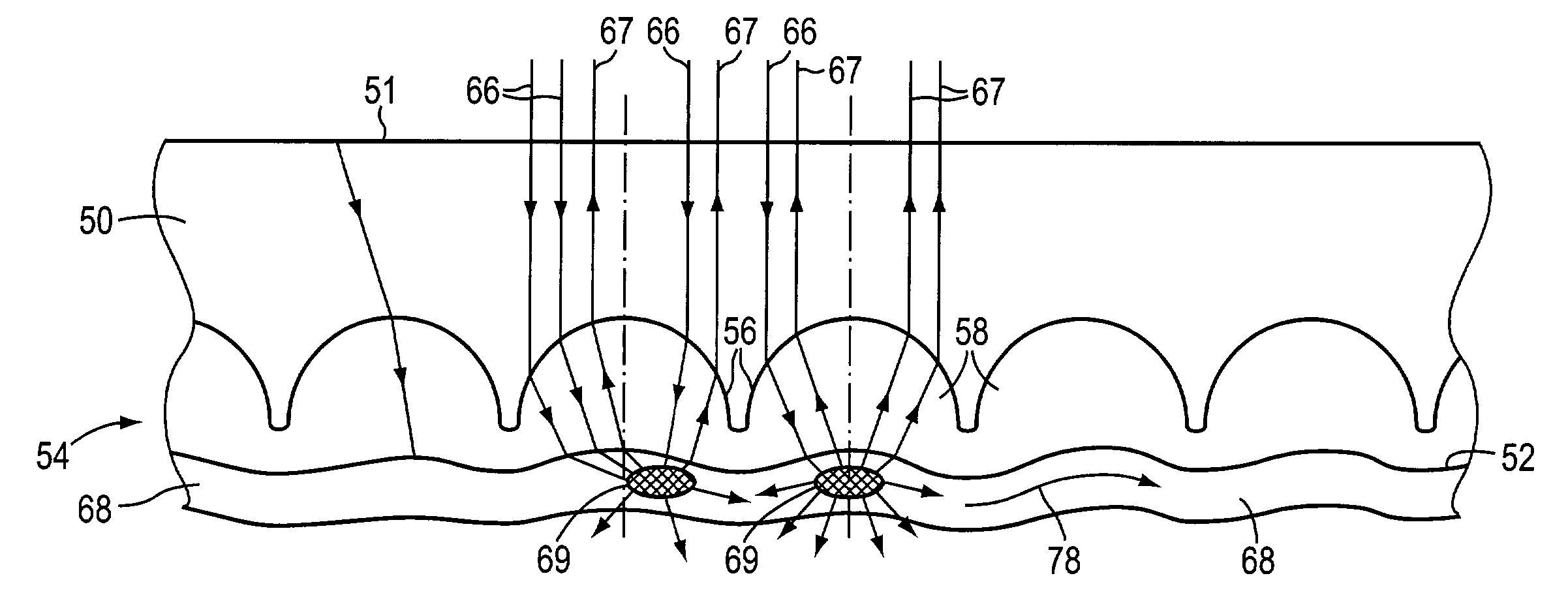
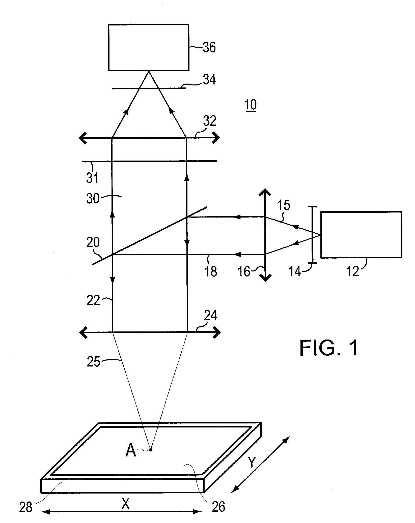
[0036]FIG. 1 illustrates one embodiment of a confocal optical scanning and imaging system for examination of biological material located on, or near, an optically active substrate shown in FIG. 3. The optically active substrate forms an important part of the optical system designed for increasing the signal-to-noise ratio of the detected optical signal.

[0037]Referring to FIG. 1, optical system 10 includes a light source 12, an entrance aperture 14, a lens 16, a dichroic mirror 20, an objective lens 24, a two or three axis translation table 28, a lens 32, an exit pinhole 34, a band pass filter or a rejection filter 31 and a detector 36. In the following embodiment, optical system 10 is arranged for the detection of fluorescent light; however, optical system 10 may also be arranged for the detection of scattered or transmitted light at the irradiation wavelength.

[0038]Light source 12 emits an excitation light beam 15, and dichroic mirror 20 directs the excitation light toward objectiv...


PUM

PropertyMeasurementUnit
thicknessaaaaaaaaaa
radiusaaaaaaaaaa
radiusaaaaaaaaaa

Abstract

A device for optical examination of biological materials using radiation of a selected wavelength includes a substrate having a first surface and a second surface opposite to the first surface. The first surface includes a dense array of micro-optical elements arranged to provide increased intensity radiation or evanescent radiation. The first surface is in close proximity to the biological material being examined.

Description

BACKGROUND OF THE INVENTION[0001]This application claims priority from U.S. Provisional Application Ser. No. 60 / 213,987, filed on Jun. 25, 2000, entitled Optically Active Substrates, which is incorporated by reference.[0002]The present invention relates to detecting and analyzing biological materials by optical scanning, and particularly relates to optical scanning or imaging of biological materials located on optically active substrates.[0003]Microarray technology enables studying complex biochemical reactions and systems at once instead of studying them individually. The technology provides a massively parallel form of analysis that increases data collection per unit time, decreases the overall time required for analysis, uses smaller sample volumes and reagent volumes and sometimes reduces disposable consumption. Although the initial cost may be high, overall the technology represents considerable savings in the time and costs of associated labor. Microarray technology became a f...

Claims


Application Information

Patent Timeline
Patent Type & Authority Patents(United States)
IPC IPC(8): G01N21/01G01N21/03G01N21/05G01N21/64G01N21/76
CPCG01N21/0303G01N21/05G01N21/6428G01N21/645G01N21/6452G01N21/648G02B3/005G02B3/0068G02B21/002G01N21/6458B01L2300/0654G01N2021/0346G01N2021/6419G01N2021/6478
Inventor MONTAGU, JEAN I.
Owner AFFYMETRIX INC
Why Eureka
Try Eureka