Semiconductor device with pixel portion and driving circuit, and electronic device

a technology of driving circuit and semiconductor device, applied in the direction of thermoelectric device, identification means, instruments, etc., can solve the problems of inability to achieve high definition and high-speed driving, and also the panel becomes larger, so as to achieve the effect of multi-functionality and higher functionality of the system

Inactive Publication Date: 2007-01-16
SEMICON ENERGY LAB CO LTD
View PDF64 Cites 46 Cited by
  • Summary
  • Abstract
  • Description
  • Claims
  • Application Information

AI Technical Summary

Benefits of technology

[0019]In the present invention, by laminating an integrated circuit that has so far been formed outside of a panel on a driving circuit on the panel, narrow framing of a system-on-panel can be realized. Furthermore, thereby the higher functionality and multi-functionality of the system can be attained.

Problems solved by technology

As a result, there are problems in that not only the high definition and high-speed driving cannot be attained but also a panel becomes larger.

Method used


Image

  • Semiconductor device with pixel portion and driving circuit, and electronic device
  • Semiconductor device with pixel portion and driving circuit, and electronic device
  • Semiconductor device with pixel portion and driving circuit, and electronic device

Examples


embodiment ] 1

[Embodiment] 1

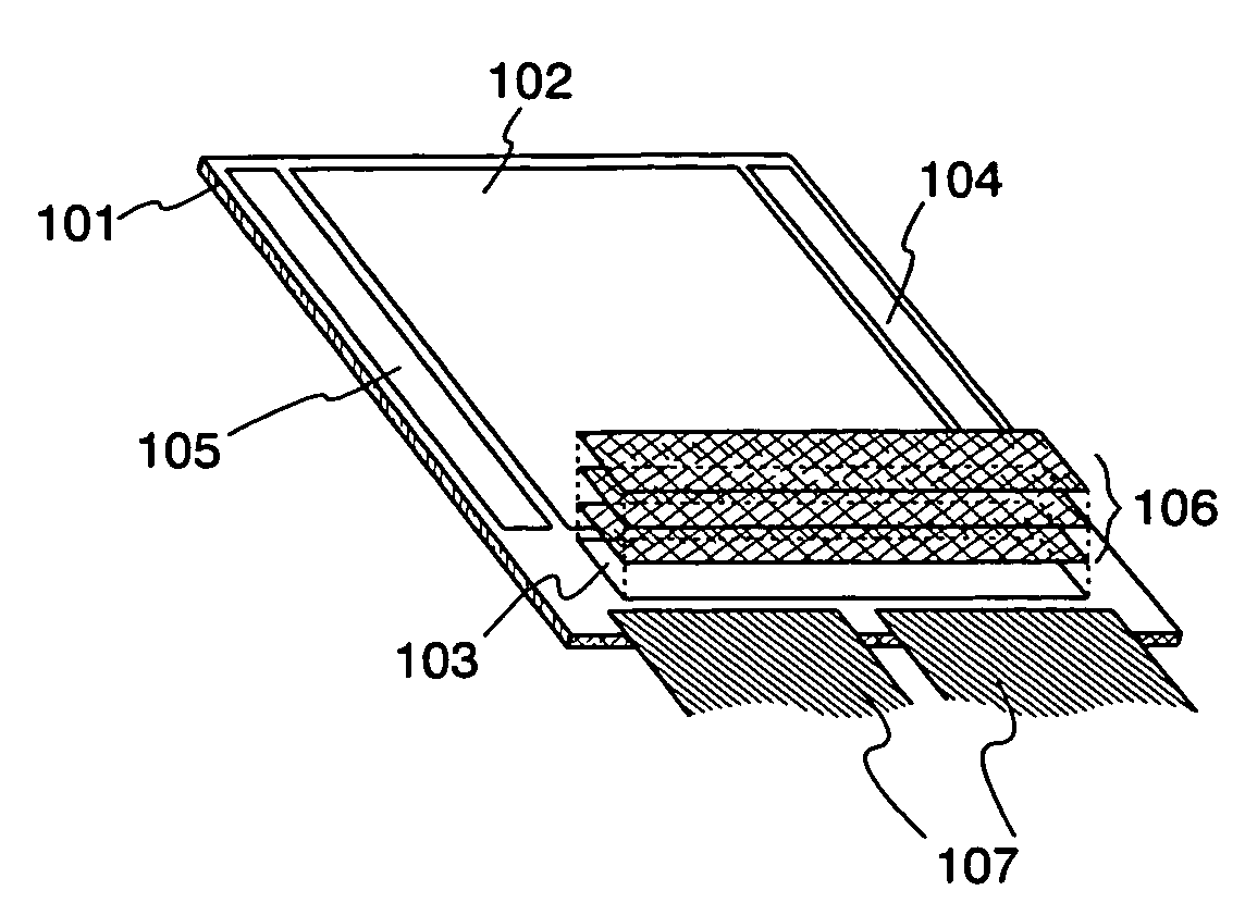
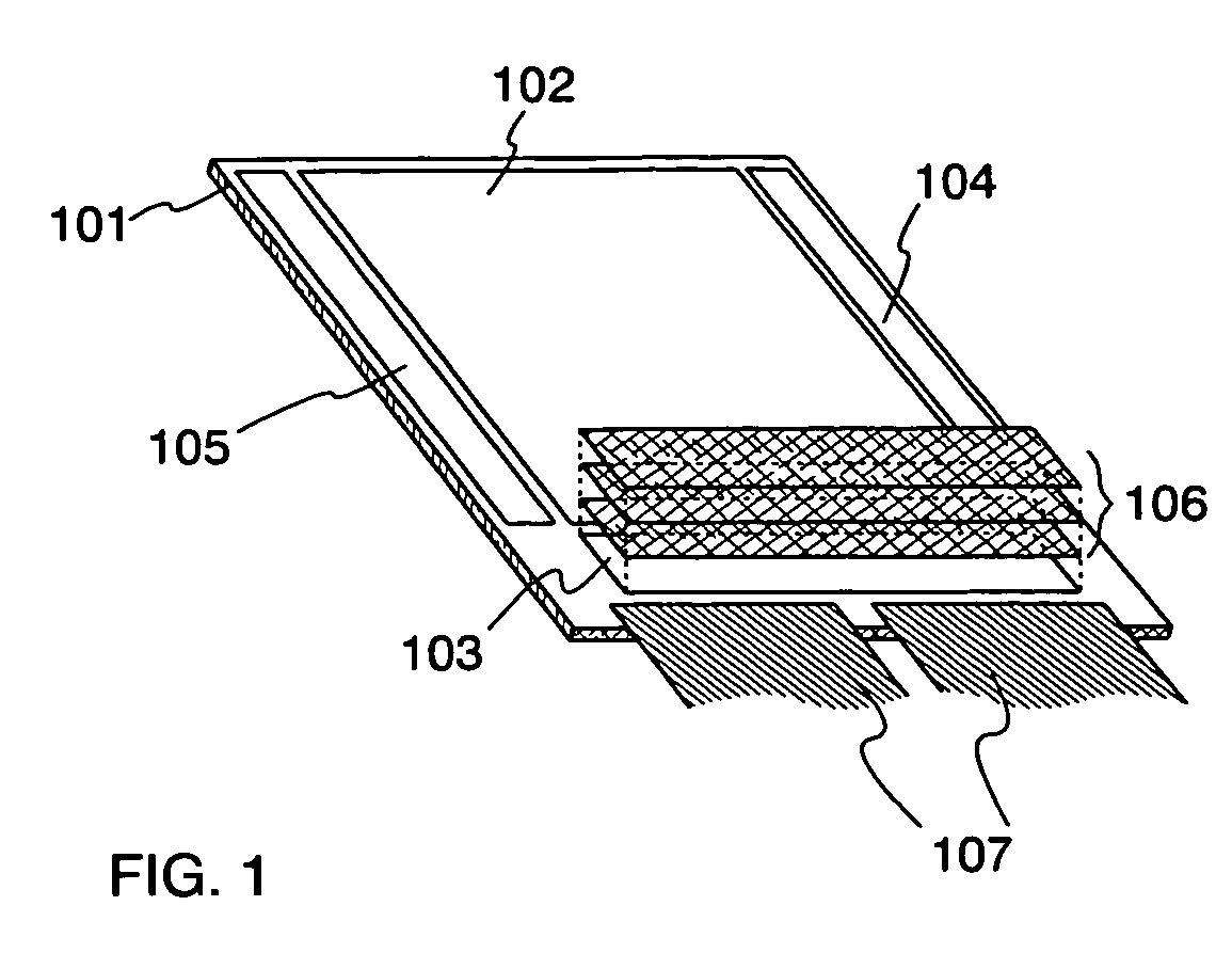
[0052]In the embodiment, a configuration comprising a display controller and a power source circuit that are indispensable in carrying out image processing to a laminated circuit of the invention will be explained with reference to a block diagram shown in FIG. 3.

[0053]That is, on desired positions on a substrate 301, a pixel portion 302, a source side driving circuit 303 that is a driving circuit and gate side driving circuits (304 and 305) are formed. On the source side driving circuit 303, a display controller 306, a frame memory A (307), a frame memory B (308) and a power source circuit 309 are formed.

[0054]Wirings on the panel are connected through a FPC310 to a signal control circuit 321 (a CPU322, a memory controller 323 and a memory 324). Furthermore, through the FPC310, a reference clock signal (CK), a synchronous signal (HSYNC & VSYNC), a video signal and the like are inputted to the display controller 306, and a reference power source and so on are inputted ...

embodiment ] 2

[Embodiment] 2

[0063]In the embodiment, a method of manufacturing a laminated integrated circuit will be detailed with reference to FIGS. 5 through 8.

[0064]In FIG. 5A, a metal layer 501, a metal oxide layer 502 and an oxide layer 503 are sequentially formed on a first substrate 500, and further thereon an element formation layer 504 is formed.

[0065]As the first substrate 500, a glass substrate, a quartz substrate, a plastic substrate, a ceramics substrate, a silicon substrate, a metal substrate or a stainless steel substrate can be used. In the embodiment, AN1OO that is a glass substrate is used.

[0066]As a material used for the metal layer 501 formed on the first substrate 500, a single layer made of an element selected from W, Ti, Ta, Mo, Nd, Ni, Co, Zr, Zn, Ru, Rh, Pd, Os, Ir and Pt or an alloy or a compound with the element as a main component or a laminate thereof, or a single layer made of a nitride thereof such as titanium nitride, tungsten nitride, tantalum nitride and molybde...

embodiment ] 3

[Embodiment] 3

[0093]In the present embodiment, a lamination structure of an integrated circuit that is different from that shown in embodiment 2 and can be obtained by, after a plurality of element formation layers are laminated, adhering a lastly laminated element formation layer on a driving circuit formed on a substrate will be explained with reference to FIGS. 9 and 10.

[0094]As shown in FIG. 9A, on a first substrate 800 a first element formation layer 902 is formed, and further to the first substrate 800, through a second adhesive layer 814, a second substrate 815 is adhered.

[0095]In the embodiment, at this time, the first substrate 800, the second adhesive layer 814 and the second substrate 815 are not peeled in a metal oxide layer 802, and on a position that does not overlap with a wiring 805 on the first element formation layer 902, a thermally conductive film 820 is formed. The thermally conductive film 820 formed here has only to be formed with a material and according to a...


PUM

PropertyMeasurementUnit
thicknessaaaaaaaaaa
thicknessaaaaaaaaaa
thicknessaaaaaaaaaa

Abstract

The present invention intends to realize a narrow frame of a system on panel. In addition to this, a system mounted on a panel is intended to make higher and more versatile in the functionality. In the invention, on a panel on which a pixel portion (including a liquid crystal element, a light-emitting element) and a driving circuit are formed, integrated circuits that have so far constituted an external circuit are laminated and formed. Specifically, of the pixel portion and the driving circuit on the panel, on a position that overlaps with the driving circuit, any one kind or a plurality of kinds of the integrated circuits is formed by laminating according to a transcription technique.

Description

TECHNICAL FIELD[0001]The present invention relates to a semiconductor device including a thin film transistor (TFT). In particular, the invention relates to a technique with which an integrated circuit is mounted on a panel including a pixel portion and a driving circuit.BACKGROUND ART[0002]In recent years, various technical developments of semiconductor devices that have thin film transistors (TFTs) formed from a semiconductor thin film (in a thickness range of substantially several to several hundreds nanometers) formed on the same substrate are forwarded.[0003]Among such semiconductor devices, a structure in which on a substrate that becomes a panel not only a pixel portion but also a driving circuit as an internal circuit are integrally formed and an external circuit is formed outside of the panel (see Patent Document 1, for embodiment) is known.[0004]On the other hand, when, in order to prepare a system on panel in which an external circuit is integrally formed, the external ci...

Claims


Application Information

Patent Timeline
Patent Type & Authority Patents(United States)
IPC IPC(8): H01L29/04H01L31/036H01L31/0376H01L31/20G02F1/1368G02F1/13G02F1/1345G02F1/1362G09F9/00H01L21/02H01L21/20H01L21/336H01L21/762H01L21/77H01L21/8234H01L21/84H01L27/00H01L27/08H01L27/088H01L27/12H01L29/786H01L51/50
CPCG02F1/13452H01L21/2007H01L21/6835H01L21/76251H01L27/1214H01L27/1266H01L27/15H01L2924/01055G02F2001/13456H01L2221/68368H01L2224/16H01L2924/01004H01L2924/01025H01L2924/01046H01L2924/01077H01L2924/01078H01L2924/01079H01L2924/04941H01L2924/3025G02F1/13454H01L2924/12044H01L2224/05009H01L2224/05025H01L2224/13025H01L2224/05001H01L2924/00014H01L27/1222H01L27/124H01L27/1274H01L2224/16145G02F1/13456H01L2924/00H01L2224/05599H01L2224/05099H10K71/50H10K50/11H10K50/15H10K50/16H10K50/17H10K50/18H10K50/81H10K50/82H10K50/171H10K59/123H10K59/126H10K59/131H10K71/00H10K71/80H10K59/1201H10K2102/103H10K2102/3031G02F1/13306G02F1/1339G02F1/1341G02F1/134309G02F1/13439G02F1/1368G02F2202/28H01L21/67196H01L21/67207H01L21/67236H01L25/0657H01L25/50H01L29/78675H01L2225/06524H01L2225/06548H01L2225/06555H01L2225/06586
Inventor YAMAZAKI, SHUNPEITAKAYAMA, TORUMARUYAMA, JUNYAGOTO, YUUGOOHNO, YUMIKOARAI, YASUYUKISHIBATA, NORIKO
Owner SEMICON ENERGY LAB CO LTD
Why Eureka
Try Eureka