Monolithic embedded integrated silicon acceleration and pressure composite sensor

A composite sensor and embedded structure technology, applied in velocity/acceleration/shock measurement, acceleration measurement using inertial force, microstructure technology, etc., can solve problems such as small gauge factor growth thickness, difficulty in improving sensor performance, and reduced device sensitivity , to achieve the effect of simplifying the processing technology, improving the utilization rate of the surface and reducing the difficulty of processing

Inactive Publication Date: 2015-01-21
SUZHOU MEILUN KAILI ELECTRONICS
View PDF5 Cites 15 Cited by
  • Summary
  • Abstract
  • Description
  • Claims
  • Application Information

AI Technical Summary

Problems solved by technology

The sensor realizes the processing of a cavity with a single crystal silicon film with a large thickness, but the process is limited to the (111) crystal plane instead of the very commonly used (100) crystal plane. The small lateral piezoresistive coefficient of this crystal plane reduces the sensitivity of the device
[0007] In the above design, the surface sacrificial layer technology, due to the small gauge factor of the polysilicon material and the limited growth thickness, and the (111) crystal plane as the process plane will also reduce the sensitivity of the device, making it difficult to improve the performance of the sensor
And the pressure sensor is separated from the acceleration sensor, occupying a large substrate area

Method used


Image

  • Monolithic embedded integrated silicon acceleration and pressure composite sensor
  • Monolithic embedded integrated silicon acceleration and pressure composite sensor
  • Monolithic embedded integrated silicon acceleration and pressure composite sensor

Examples


Embodiment Construction

[0034] In order to make the above objects, features and advantages of the present invention more obvious and comprehensible, the present invention will be further described in detail below in conjunction with the accompanying drawings and specific embodiments.

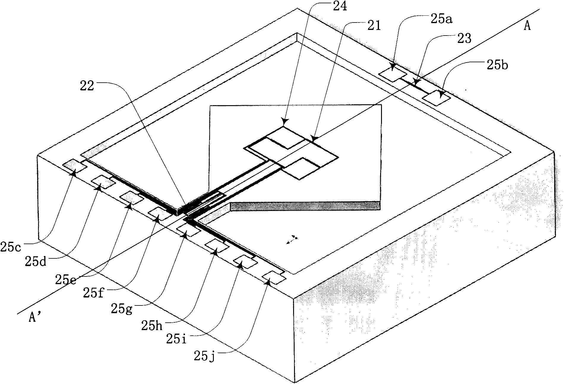
[0035] like Figure 1A ~ Figure 1B As shown, the monolithic embedded structure integrated silicon acceleration and pressure composite sensor includes a pressure sensor force-sensitive resistor 21, an acceleration sensor force-sensitive resistor 22, a temperature-sensitive resistor 23, metal leads 24, and welding electrodes 25a-25j.

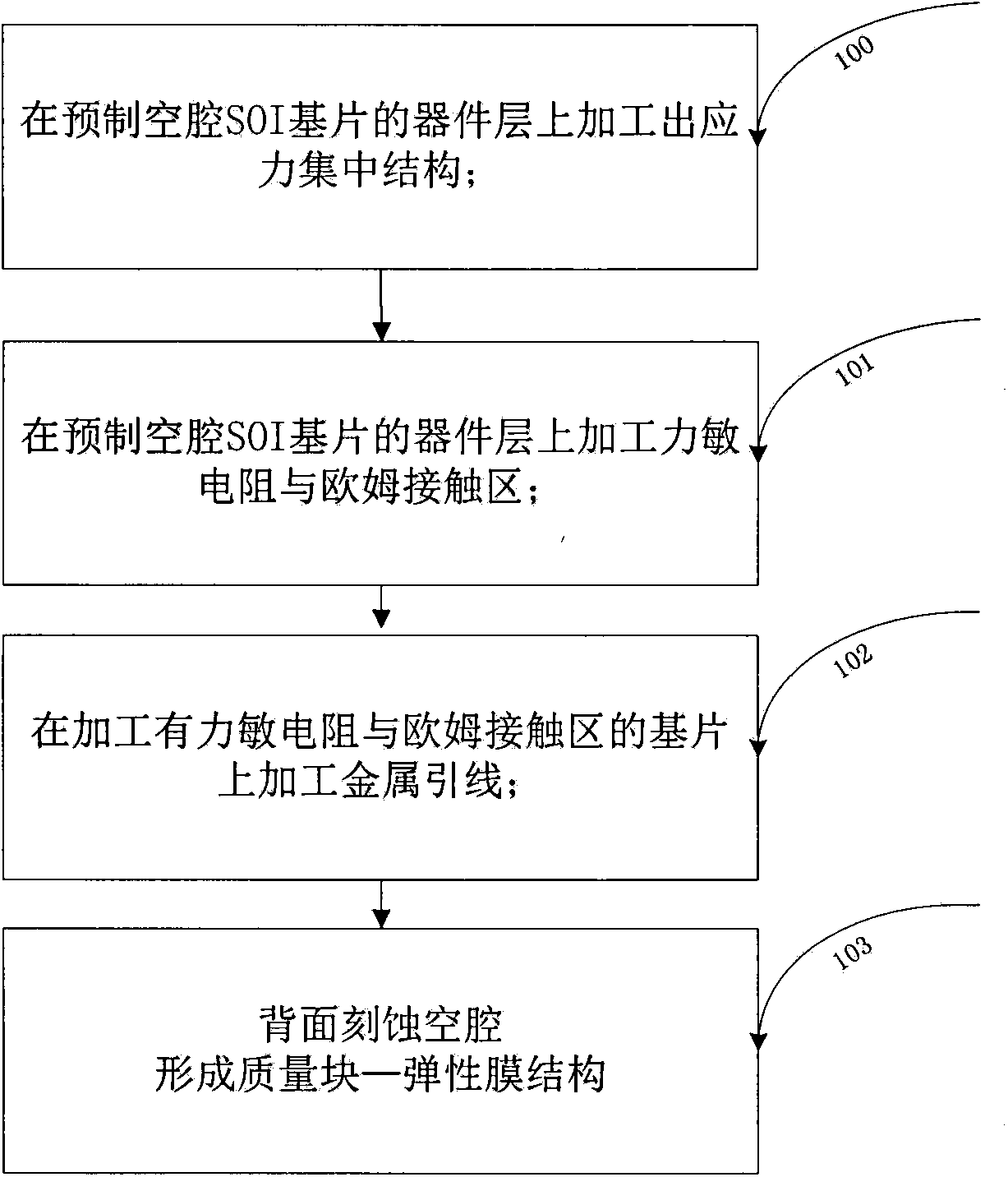
[0036] figure 2 It is a flow chart of the processing steps of the single-chip embedded structure integrated silicon acceleration and pressure composite sensor of the present invention, including the processing step of the stress concentration structure (optional), and the processing step 101 of the force sensitive resistor: the device on the prefabricated cavity SOI substrate A force-sen...


PUM


Abstract

The invention belongs to a micro electro mechanical (MEMS) processing field and relates to a monolithic embedded integrated silicon acceleration and pressure composite sensor. The objective of the invention is to provide the monolithic embedded integrated silicon acceleration and pressure composite sensor and a typical processing method for manufacturing the sensor. The composite sensor is of an integrated structure. An accelerometer includes a mass block-elastic diaphragm structure with a force sensitive resistor; a pressure gauge includes a pressure sensitive diaphragm with a force sensitive resistor and a sealed prefabricated cavity. The method includes the following steps of: a stress concentration structure processing step which is optional; a sensitive resistor processing step; a metal lead layer processing step; and accelerometer mass block-elastic diaphragm structure processing step. According to the monolithic embedded integrated silicon acceleration and pressure composite sensor of the invention, the accelerometer and the pressure gauge are designed in the same area, and therefore, the area of a chip can be saved, and high sensitivity can be realized when size is small. The sensor fabricated through adopting the method has functions of a pressure gauge and an accelerometer.

Description

technical field [0001] The invention relates to the field of micro-electronic machinery (MEMS) processing, in particular to a single-chip embedded structure integrated silicon acceleration and pressure composite sensor. Background technique [0002] tpms acceleration sensors and pressure sensors are widely used in various fields such as aerospace, aviation, navigation, petrochemical, automobile manufacturing, power machinery, biomedical engineering, meteorology, geology, and seismic measurement. Micro-electro-mechanical (MEMS) piezoresistive sensors are sensor chips manufactured using the piezoresistive effect of single crystal silicon through MEMS processing technology. Because of its small size, high precision, low cost, and mass production, it has wide application space and market prospects. [0003] The piezoresistive MEMS sensor has the advantages of good output linearity, high sensitivity, wide operating temperature range, and good dynamic response characteristics. I...

Claims


Application Information

Patent Timeline
Patent Type & Authority Applications(China)
IPC IPC(8): G01P15/12G01L1/20G01L9/02B81B7/00B81C1/00
Inventor 张扬熙高成臣杨琛琛孟凡瑞
Owner SUZHOU MEILUN KAILI ELECTRONICS
Why Eureka
Try Eureka