
Etchant, method for roughening copper surface and method for producing printed wiring board

a technology of copper surface and printed wiring board, which is applied in the direction of paper/cardboard articles, cable/conductor manufacturing, and metal adhesion improvement of insulating substrates. it can solve the problems of pink ring on the conductive pattern layer, increase the manufacturing cost first process encounter serious problems. , to achieve the effect of reducing the number of steps in manufacturing of printed wiring board, increasing acid resistan

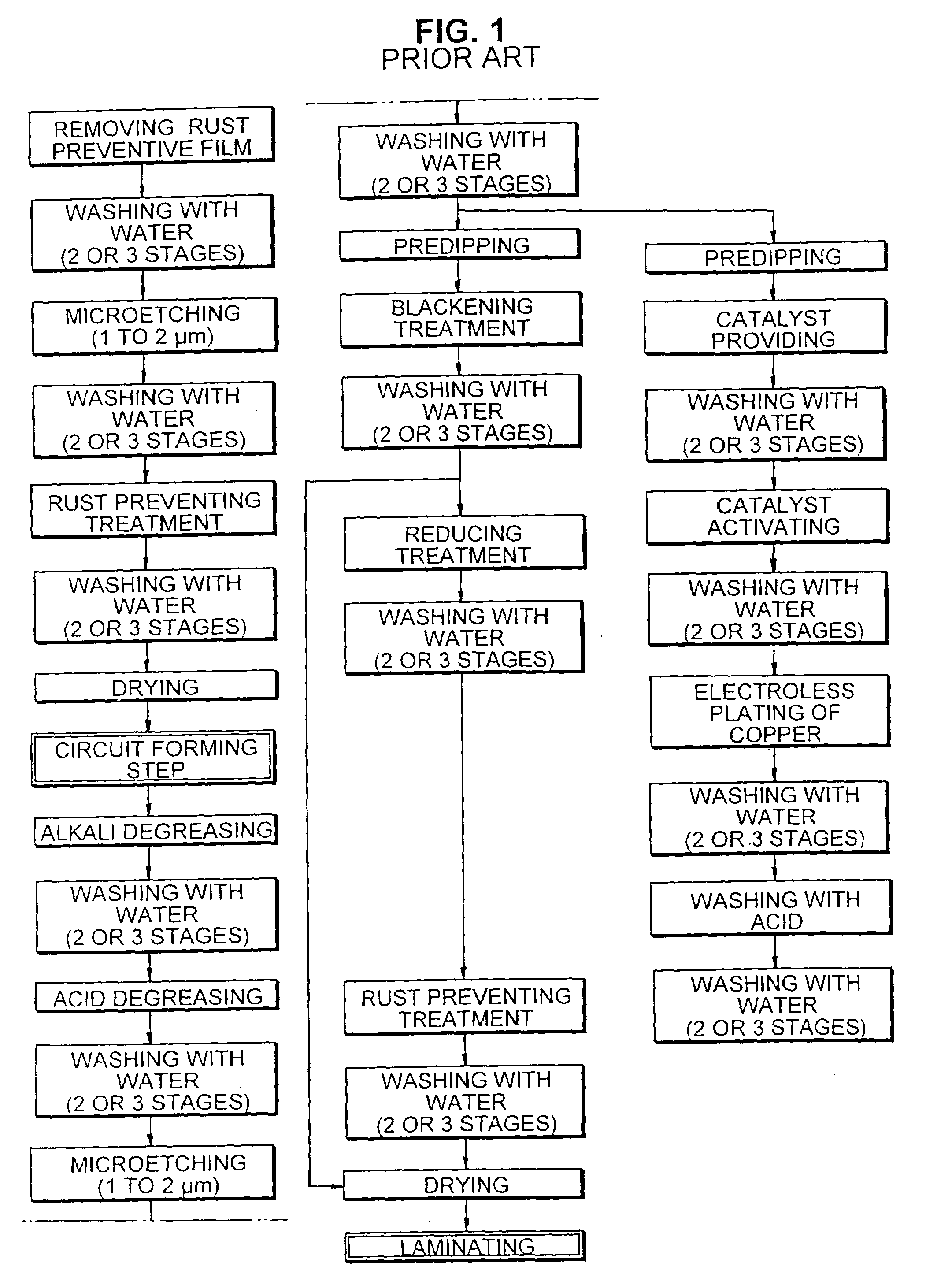
Inactive Publication Date: 2007-03-13
EBARA DENSAN KK
View PDF22 Cites 7 Cited by
  • Summary
  • Abstract
  • Description
  • Claims
  • Application Information

AI Technical Summary

Benefits of technology

[0009]Accordingly, it is an object of the present invention to provide an etching solution or etchant which is capable of providing a copper conductive pattern layer with a roughened surface exhibiting increased acid resistance.
[0010]It is another object of the present invention to provide a method for roughening a copper surface which is capable of firmly joining a copper conductive pattern and an outer layer material to each other to reduce the number of steps in manufacturing of a printed wiring board.
[0011]It is a further of the present invention to provide a method for producing a printed wiring board which is capable of preventing a defect such as a pink ring or the like from occurring on a conductive pattern layer.

Problems solved by technology

Unfortunately, the first process encounters a serious problem.
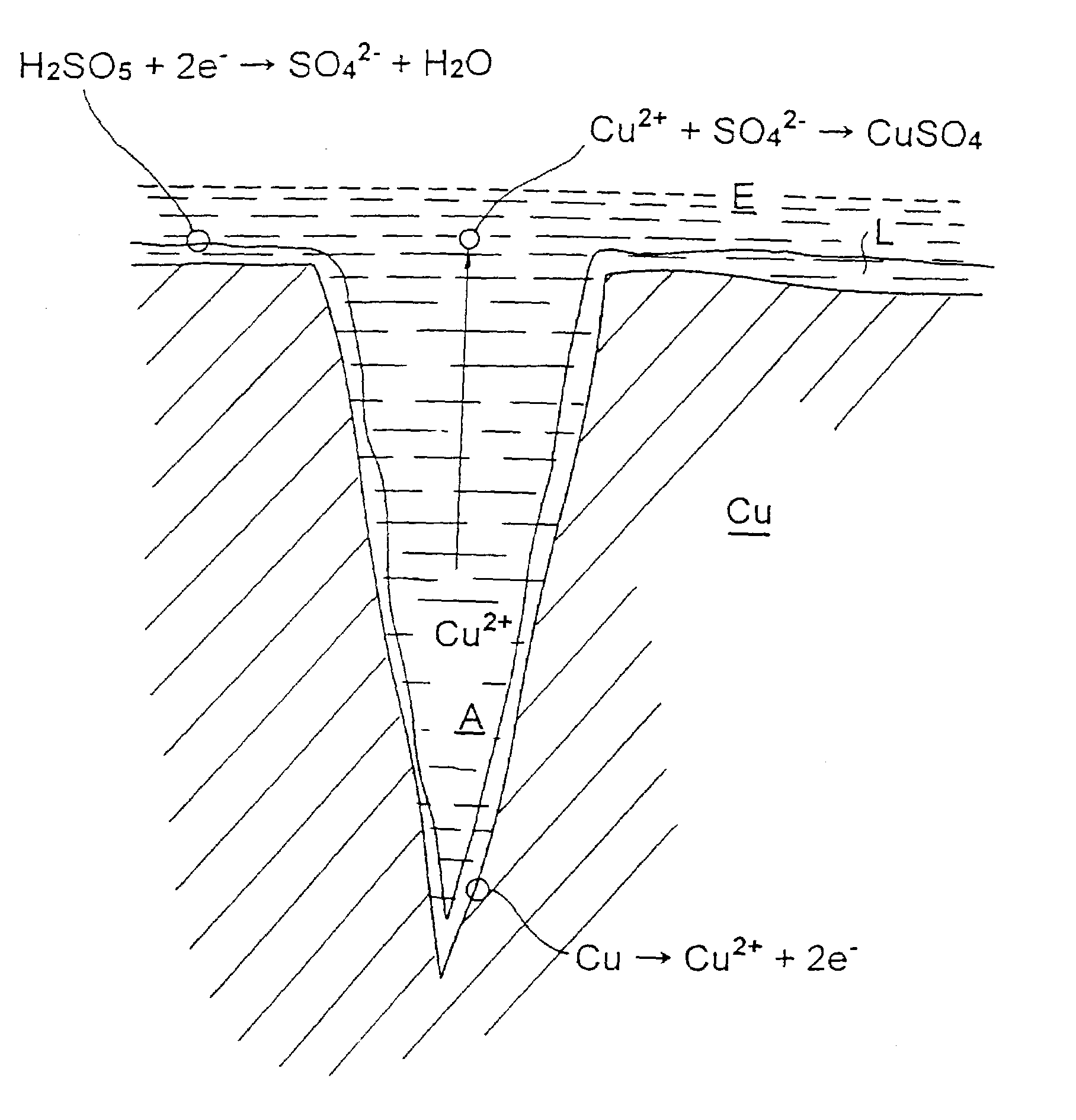
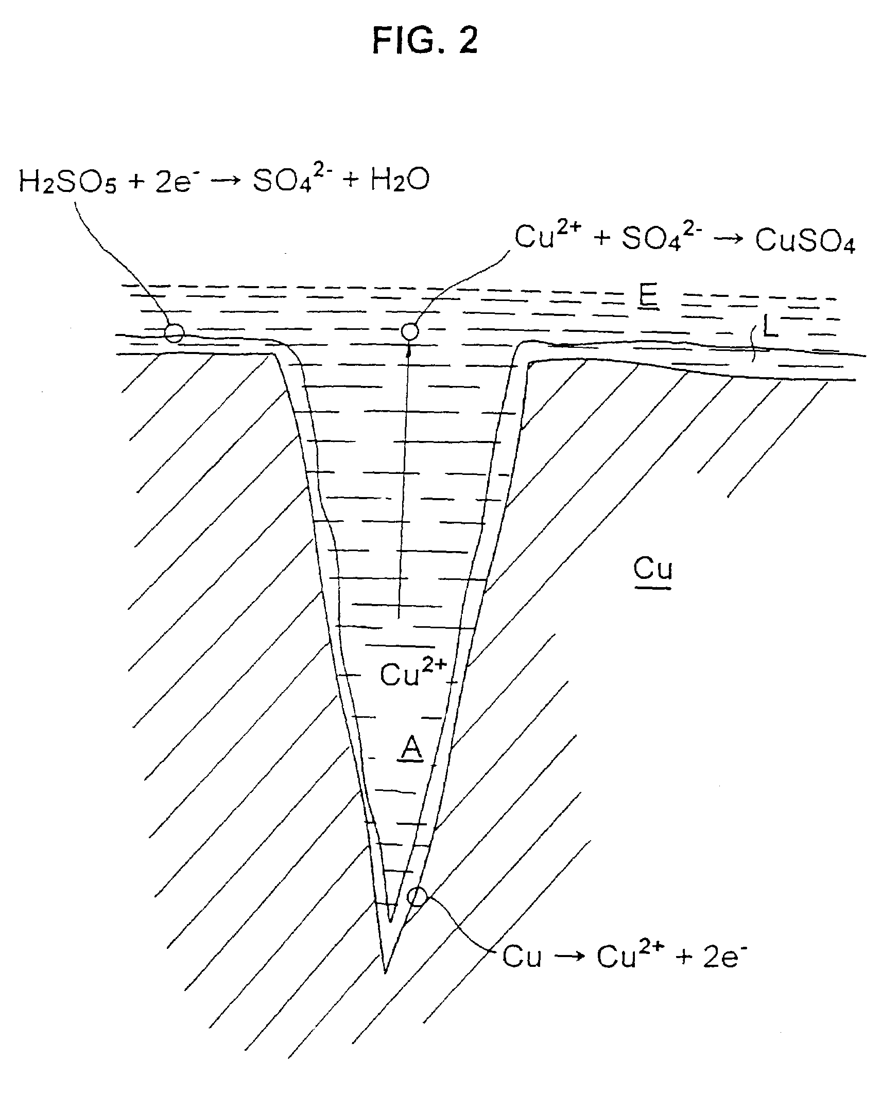
Thus, when the copper oxide of the copper conductive pattern layer is exposed on an inner surface of the through-holes due to formation of the through-holes, dipping of the copper conductive pattern layer in an etching solution or etchant during the subsequent electroplating causes the copper oxide to react with sulfuric acid in the etchant, to thereby be dissolved in the form of copper sulfate in the etchant, resulting in a defect called a pink ring occurring on the conductive pattern layer.
Also, it has another disadvantage of causing an increase in manufacturing cost of a printed wiring board because a reducing agent for the reduction is expensive.

Method used


Image

  • Etchant, method for roughening copper surface and method for producing printed wiring board
  • Etchant, method for roughening copper surface and method for producing printed wiring board
  • Etchant, method for roughening copper surface and method for producing printed wiring board

Examples


example 1

[0051]First, a first aqueous etching solution or etchant having such a composition as shown in Table 1 described below was prepared.

[0052]

TABLE 1(Temperature: 20° C.)H2O225 g / lH2SO490 g / l

[0053]A surface of a copper-clad laminate made of epoxy resin filled with a glass fabric was dipped in the thus-prepared etchant for 1 minute to remove a rust preventive film from the surface. Then, the laminate was dipped for 5 minutes in a second etching solution or etchant having such a composition as shown in Table 2 described below, to thereby be subjected to etching, resulting in the surface of the laminate being roughened.

[0054]

TABLE 2(Temperature: 25° C.)H2O280g / lH2SO490g / lBTA5g / lNaCl0.2g / l

[0055]Then, the copper surface of the copper-clad laminate thus etched was observed by means of a scanning electron microscope (SEM). As a result, it was found that the surface is formed thereon with fine acicular protrusions as shown in FIGS. 4A and 4B. Also, a section of the copper-clad laminate was obse...

example 2

[0057]A surface of a copper-clad laminate made of epoxy resin filled with a glass fabric was dipped in the etchant shown in Table 1 for 1 minute to remove a rust preventive film from the surface as in the Example 1. Then, the laminate was dipped for 5 minutes in a third etching solution or etchant having such a composition as shown in Table 3 described below, resulting in the surface of the laminate being roughened.

[0058]

TABLE 3(Temperature: 25° C.)K2SO5250g / lH2SO490g / lBTA5g / lNaCl0.2g / l

[0059]As will be noted from Tables 2 and 3, the third etchant was substantially the same as the second etchant except that potassium peroxomonosulfate (K2SO5) was substituted for hydrogen peroxide (H2O2).

[0060]The copper surface was likewise subjected to SEM observation. As a result, it was found that the surface is formed thereon with such protrusions as shown in FIGS. 7A and 7B, resulting in being roughened. Comparison of Example 2 with Example 1 indicated that roughening of the copper surface in Ex...

example 3

[0062]A surface of a copper-clad laminate made of epoxy resin filled with a glass fabric was dipped for 1 minute in the etchant shown in Table 1 to remove a rust preventive film from the surface as in Examples 1 and 2 described above. Then, the laminate was dipped for 5 minutes in a fourth etching solution or etchant having such a composition as shown in Table 4 described below, resulting in the surface of the laminate being roughened.

[0063]

TABLE 4(Temperature: 25° C.)H2O280g / lHClO4150g / lBTA5g / lNaCl0.2g / l

[0064]As will be noted from Tables 2 and 4, the fourth etchant was substantially the same as the second etchant except that perchloric acid (HClO4) was substituted for sulfuric acid (H2SO4). The copper surface was likewise subjected to observation by means of the SEM. As a result, it was found that the surface is formed thereon with such protrusions as shown in FIGS. 8A and 8B, resulting in being roughened.

[0065]Then, the copper-clad laminate having the surface thus roughened was li...


PUM

PropertyMeasurementUnit
Lengthaaaaaaaaaa
Timeaaaaaaaaaa
Concentrationaaaaaaaaaa

Abstract

An etchant and a method for roughening a copper surface each capable of permitting copper with roughened surface which exhibits acid resistance and permits a copper conductive pattern and an outer layer material to be firmly bonded to each other therethrough in manufacturing of a printed wiring board to simplify the manufacturing. The etchant may contain an oxo acid such as sulfuric acid, peroxide such as hydrogen peroxide and an auxiliary component such as an azole and chlorine. The azole may comprise benzotriazole (BTA). The chlorine may be in the form of sodium chloride (NaCl). The etchant permits a copper surface to be roughened in an acicular manner.

Description

[0001]This a divisional application of U.S. patent application Ser. No. 08 / 901,700, filed Jul. 28, 1997, now U.S. Pat. No. 6,544,436.BACKGROUND OF THE INVENTION[0002]This invention relates to techniques of etching a copper foil or copper plate, and more particularly to an etching solution or etchant for roughening a surface of a copper foil or copper plate so that the surface has acicular protrusions, a method for roughening a copper surface and a method for producing a printed wiring board in which a defect such as a pink ring or the like can be prevented from occurring and the number of manufacturing steps can be reduced.[0003]A multi-layer printed wiring board has been conventionally made by laminating an inner layer material, an outer layer material and prepregs on each other. A copper-clad laminate on which a copper foil is laminated is used as the inner layer material and the like. In general, manufacturing of such a multi-layer printed wiring board is carried out in such a ma...

Claims


Application Information

Patent Timeline
IPC IPC(8): C23F1/34C23F1/18H05K3/38H05K3/46
CPCC23F1/18H05K3/383H05K2203/124H05K2203/0796H05K3/4611H05K3/46
Inventor MORIKAWA, YOSHIHIKOSENBIKI, KAZUNORIYAMAZAKI, NOBUHIRO
Owner EBARA DENSAN KK
Learn More