Use of waveguide grating couplers in an optical mux/demux system

a technology of waveguide grating and optical mux, which is applied in the direction of optics, instruments, optical light guides, etc., can solve the problems of incompatibility of gratings and awgs with multi-mode optical fibers, inconvenient solution, and drawbacks of wdm technologies

Active Publication Date: 2007-03-20
CISCO TECH INC
View PDF8 Cites 48 Cited by
  • Summary
  • Abstract
  • Description
  • Claims
  • Application Information

AI Technical Summary

Problems solved by technology

However, there are drawbacks associated with these WDM technologies.
Many of these systems, such as the MZI, Bragg gratings and AWG are incompatible with multi-mode optical fibers.
Thin film filters and bulk diffraction grating can be used with multi-mode fibers, but this requires use of free-space optical systems, which require more parts and precise alignment, resulting in costly solutions.
F

Method used


Image

  • Use of waveguide grating couplers in an optical mux/demux system
  • Use of waveguide grating couplers in an optical mux/demux system
  • Use of waveguide grating couplers in an optical mux/demux system

Examples


Embodiment Construction

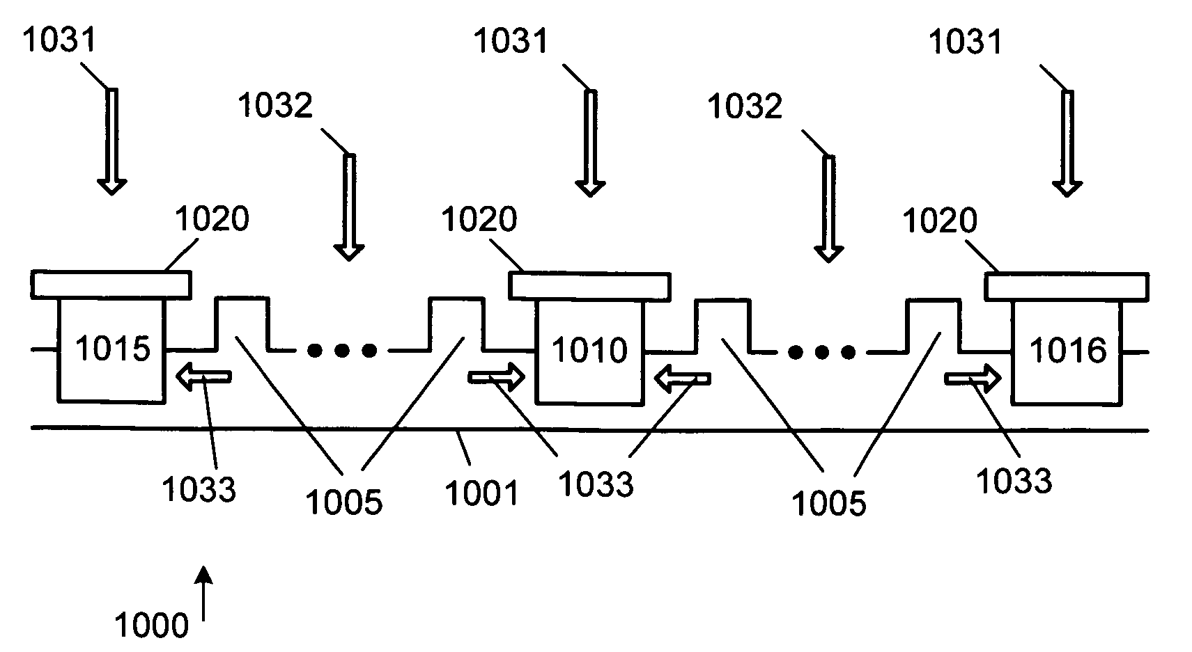
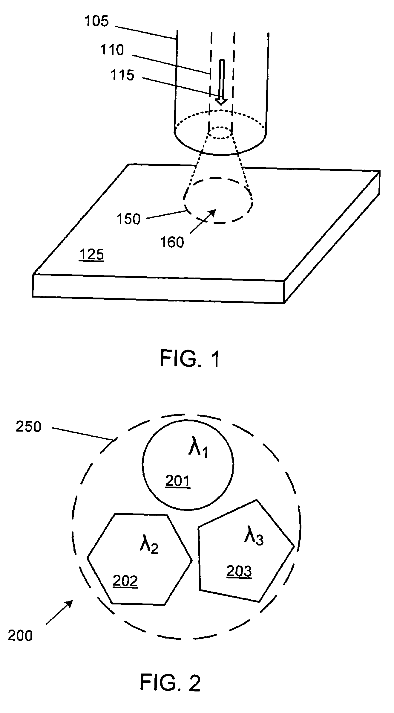
[0026]FIG. 1 is a diagram of an oblique view of optical fiber 105 optically coupled to grating coupler demultiplexer 160, according to one embodiment of the present invention. Grating coupler demultiplexer 160 is made of several waveguide grating couplers disposed on substrate 125. The substrate 125 can be an integrated circuit, a chip, a die or a wafer. Various types of Group IV semiconductors, such as silicon, germanium, diamond, silicon carbide, silicon germanium, or strained silicon can be used. Additionally, compound semiconductors such as: gallium arsenide, gallium nitride, indium phosphide, indium gallium arsenide phosphide, indium gallium arsenide, or other related Group III-V or Group II-VI compound semiconductors can be used as a substrate. Alternatively, dielectric substrates, such as quartz, sapphire, silica, or other glasses can be used. A combination of semiconductor and dielectric is also possible, such as a silicon-on-insulator (SOI) wafer or a silicon-on-sapphire (S...


PUM


Abstract

A group of waveguide grating couplers is disposed on a semiconductor substrate. The grating couplers are all within a spot illuminated on the substrate by a light from an optical fiber. The light propagating in the fiber is wavelength division multiplexed (WDM) and consists of several channels. Within the group of grating couplers, at least one grating coupler is designed to be tuned to each of the channels. The group of grating couplers demultiplexes the channels propagating in the fiber. A group of waveguide grating couplers can also be used to multiplex several channels of light into an optical fiber. Single mode and multimode fiber can be used to carry the multiplexed channels of light in an optical multiplexing and demultiplexing system.

Description

CROSS-REFERENCE TO RELATED APPLICATIONS[0001]This application claims priority from U.S. Provisional application No. 60 / 604,797 filed Aug. 26, 2004.FIELD OF THE INVENTION[0002]The present invention relates to the use of waveguide grating couplers in an optical multiplexing and demultiplexing system, where the multiplexed signals propagate through optical fibers.BACKGROUND OF THE INVENTION[0003]Optical fibers have been widely used in high speed communications links. Optical links using fiber optics have many advantages compared to electrical links: large bandwidth, high noise immunity, reduced power dissipation and minimal crosstalk. Fiber optic communications links can have data transmission capacity in the terabit per second range. In communications systems where optical fibers are used to transport optical communications signals, various optoelectronic devices are used to control, modify and process the optical signals.[0004]Wavelength division multiplexing (WDM) is an essential te...

Claims


Application Information

Patent Timeline
IPC IPC(8): G02B6/34G02B6/26G02B6/42
CPCG02B6/4204G02B6/34G02B6/30G02B6/4214
Inventor GUNN, III, LAWRENCE C.
Owner CISCO TECH INC
Why Eureka
Try Eureka