Epitaxially grown nitride-based compound semiconductor crystal substrate structure with low dislocation density

a compound semiconductor and crystal substrate technology, applied in the direction of crystal growth process, semiconductor laser, sport apparatus, etc., can solve the problems of difficult to realize, complex and time-consuming process of forming the patterned siosub>2 /sub>mask, and difficult to realize a desired crystal growth, etc., to and reduce the dislocation or defect density level

Inactive Publication Date: 2007-03-27
SUMITOMO CHEM CO LTD
View PDF23 Cites 29 Cited by
  • Summary
  • Abstract
  • Description
  • Claims
  • Application Information

AI Technical Summary

Benefits of technology

[0016]It is a further object of the present invention to provide a novel method of forming an epitaxially grown nitride-based compound semiconductor crystal substrate structure, wherein at least an upper region of the substrate structure has a reduced dislocation or defect density level which is generally lower than a minimum-required low density range for numerous applications to a variety of advanced nitride-based compound semiconductor devices such as the laser diode and light-emitting diodes.
[0032]It is yet an additional object of the present invention to provide a novel nitride-based compound semiconductor device formed over an epitaxially grown single-layered nitride-based compound semiconductor crystal substrate, wherein an entirety of the single-layered substrate generally has a reduced dislocation or defect density level which is generally lower than a minimum-required low density range for numerous applications to a variety of advanced nitride-based compound semiconductor devices such as the laser diode and light-emitting diodes.

Problems solved by technology

It has been known to the persons skilled in the art that it is not easy to realize a desired crystal growth in bulk-form or single-layered form of the nitride-based compound semiconductor crystal, while such a single-layered nitride-based compound semiconductor crystal substrate would be desirable, wherein an entirety of the substrate comprises a single layer of a nitride-based compound semiconductor crystal.
This lattice-mismatch between sapphire and nitride-based compound semiconductor is so large as making it difficult to realize a desirable epitaxial growth of the nitride-based compound semiconductor crystal directly on the surface of the sapphire single crystal.
Those sequential processes for forming the patterned SiO2 mask are complicated and time-consuming processes, and also need highly accurate advanced micro-lithography techniques.
The above-described growth techniques, utilizing the patterned SiO2 mask, may also include numerous heat treatment processes and cleaning processes, and cause pollution and damage to the substrate due to handling.
Notwithstanding, the above-described growth techniques, utilizing the patterned SiO2 mask, result in still higher dislocation density levels than the desired low levels for practical applications to the advanced laser diode and / or light emitting diode.
Namely, the above-described growth techniques do not satisfy the actual requirements for the practical applications.

Method used


Image

  • Epitaxially grown nitride-based compound semiconductor crystal substrate structure with low dislocation density
  • Epitaxially grown nitride-based compound semiconductor crystal substrate structure with low dislocation density
  • Epitaxially grown nitride-based compound semiconductor crystal substrate structure with low dislocation density

Examples


example 1

[0111]A single crystal sapphire substrate was prepared, which has a diameter of 2 inches and a surface with C-plane. An undoped epitaxial GaN layer with a thickness of 400 nanometers was deposited on the C-plane of the single crystal sapphire substrate by MOCVD using trimethyl gallium (TMG) and NH3 as source gases. A titanium film with a thickness of 20 nanometers was formed by evaporation on the undoped epitaxial GaN layer. The substrate was subjected to an X-ray diffraction measurement, a result of which is shown in FIG. 3. It was observed that the titanium film has a crystal orientation to [0001].

[0112]The substrate was put into a reaction chamber of MOCVD system. An ammonia gas containing 20% of H2 gas was continuously supplied to the chamber. A heat treatment was carried out at 1050° C. for 30 minutes in the presence of a gas flow of NH3 and H2, whereby the titanium film is nitrated to form a titanium nitride film. The heat-treated substrate was again subjected to an X-ray diff...

example 2

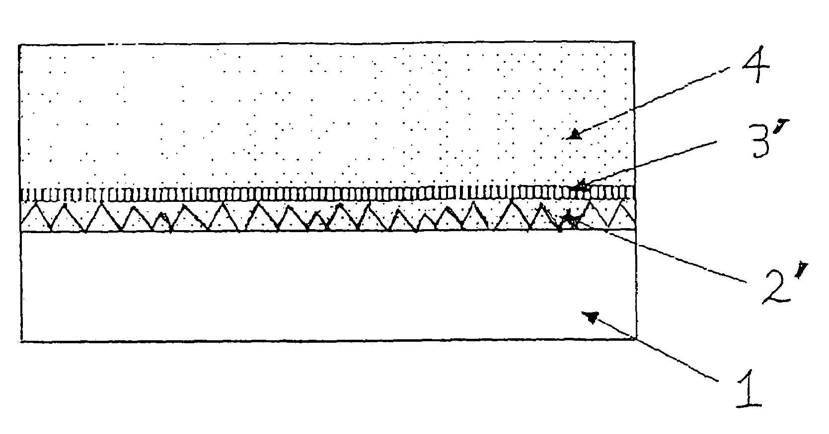
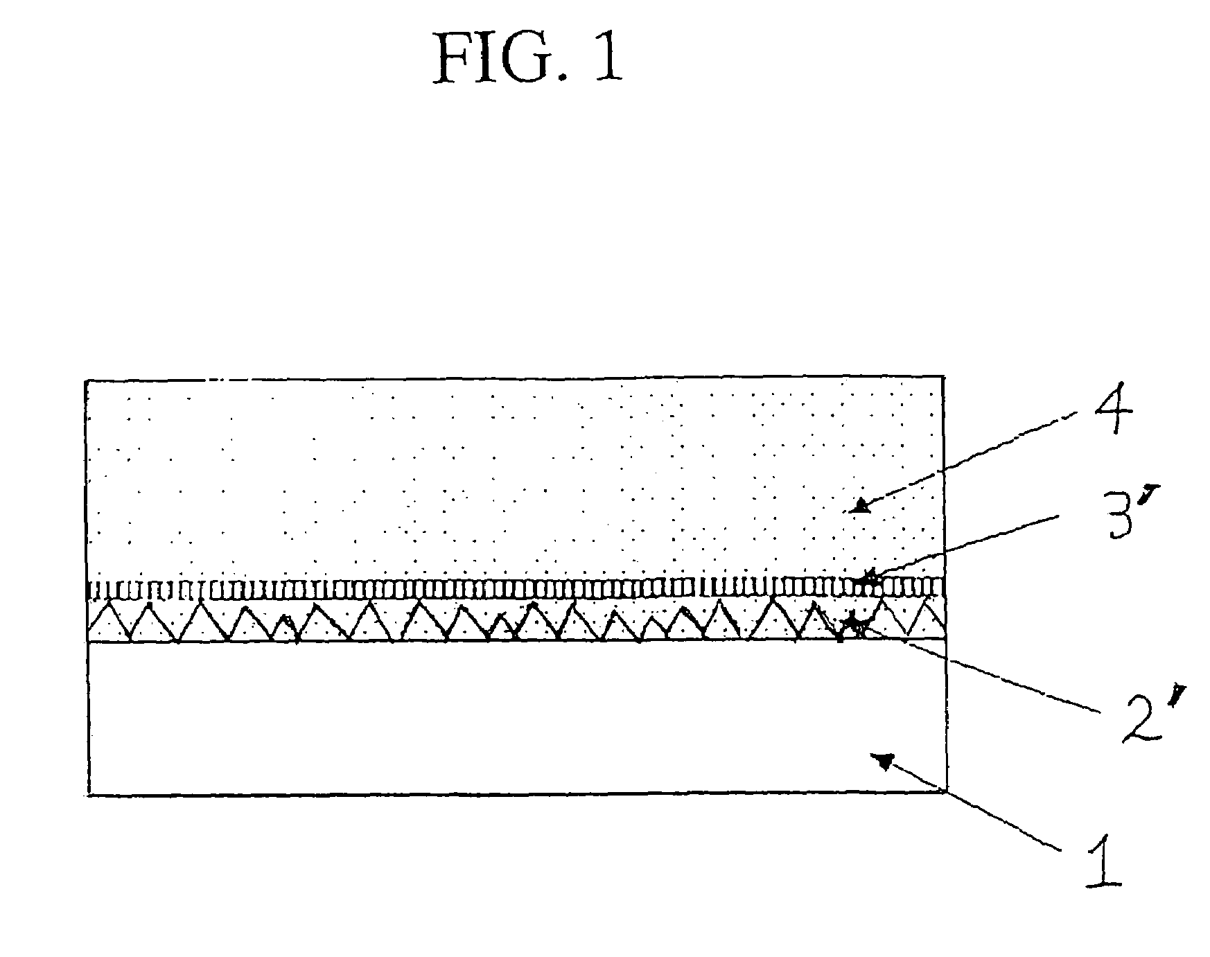
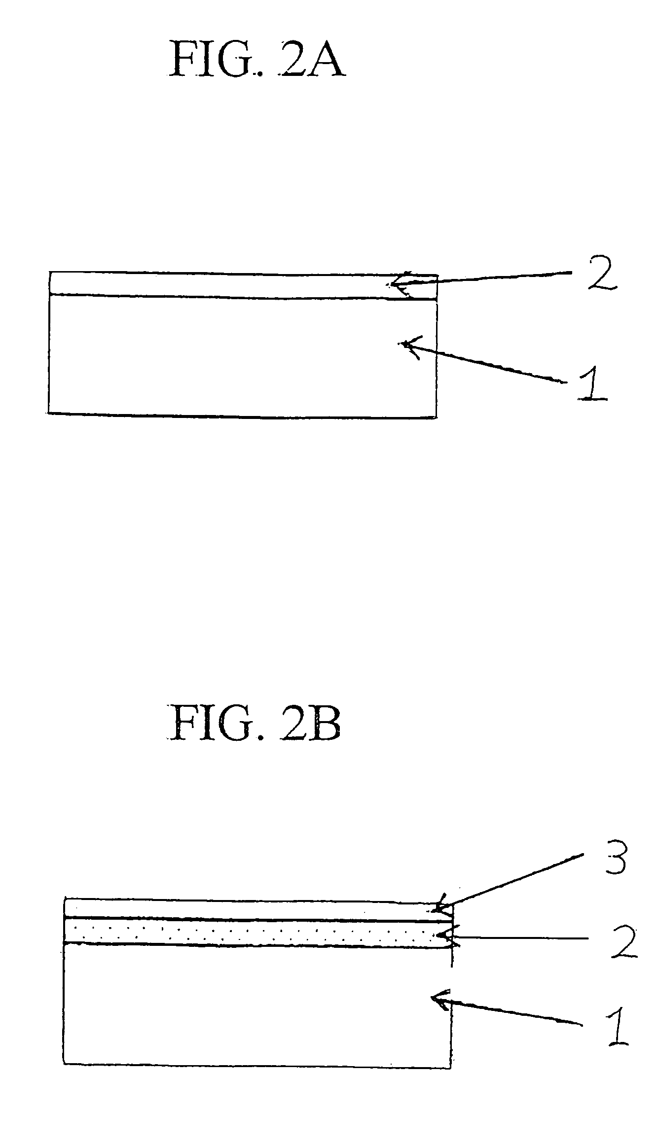
[0113]With reference to FIG. 2A, a single crystal sapphire substrate 1 was prepared, which has a diameter of 2 inches and a surface with C-plane. An undoped epitaxial GaN layer 2 with a thickness of 400 nanometers was deposited on the C-plane of the single crystal sapphire substrate 1 by MOCVD using trimethyl gallium (TMG) and NH3 as source gases.

[0114]With reference to FIG. 2B, a titanium film 3 with a thickness of 20 nanometers was formed by evaporation on the undoped epitaxial GaN layer 2.

[0115]With reference to FIG. 2C, the substrate was put into a reaction chamber of MOCVD system. An ammonia gas containing 20% of H2 gas was continuously supplied to the chamber. A heat treatment was carried out at 1050° C. for 30 minutes in the presence of a gas flow of NH3 and H2, whereby the titanium film 3 is nitrated to form a titanium nitride film 3′.

[0116]With reference to FIG. 2D, subsequently, without exposing the substrate to an outside atmosphere, the substrate was subjected to a furth...

example 3

[0122]A single crystal sapphire substrate was prepared, which has a diameter of 2 inches and a surface with C-plane. An undoped epitaxial GaN layer with a thickness of 500 nanometers was deposited on the C-plane of the single crystal sapphire substrate by MOCVD using trimethyl gallium (TMG) and NH3 as source gases. A titanium film with a thickness of 25 nanometers was formed by evaporation on the undoped epitaxial GaN layer. The substrate was put into a reaction chamber of MOCVD system. An argon gas containing 20% of H2 gas was continuously supplied to the chamber. A first heat treatment was carried out at 1050° C. for 10 minutes in the presence of a gas flow of Ar and H2. Subsequently, a second heat treatment was carried out at 1050° C. for 30 minutes in the presence of a gas flow of NH3 and H2. Thereafter, without exposing the substrate to an outside atmosphere, the substrate was subjected to a further epitaxial growth 1050° C. with supplying trimethyl gallium (TMG) and NH3 as sou...


PUM

PropertyMeasurementUnit
depthaaaaaaaaaa
porosity rateaaaaaaaaaa
dislocation densityaaaaaaaaaa

Abstract

A metal layer is formed directly on a nitride-based compound semiconductor base layer over a substrate body. The metal layer includes at least one metal exhibiting an atomic interaction, with assistance of a heat treatment, to atoms constituting the base layer to promote removal of constitutional atoms from the base layer, whereby pores penetrating the metal layer are formed, while many voids are formed in the nitride-based compound semiconductor base layer. An epitaxial growth of a nitride-based compound semiconductor crystal is made with an initial transient epitaxial growth, which fills the voids, and a subsequent main epitaxial growth over the porous metal layer.

Description

CROSS REFERENCE TO RELATED APPLICATIONS[0001]This application is a division of application Ser. No. 10 / 150,960, filed on May 21, 2002, and issued as U.S. Pat. No. 6,812,051, on Nov. 2, 2004 the entire contents of which are hereby incorporated by reference.BACKGROUND OF THE INVENTION[0002]1. Field of the Invention[0003]The present invention relates to a method of forming an epitaxially grown nitride-based compound semiconductor crystal substrate structure with a reduced dislocation density, and a nitride-based compound semiconductor crystal substrate structure with a reduced dislocation density.[0004]2. Description of the Related Art[0005]Gallium nitride-based compound semiconductors are attractive to persons skilled in the art for a wide variety of applications to various semiconductor devices, for example, light emitting diodes such as a blue-color light emitting diode and laser diodes. The gallium nitride-based compound semiconductors include various compound semiconductors includ...

Claims


Application Information

Patent Timeline
Patent Type & Authority Patents(United States)
IPC IPC(8): H01L29/20H01L31/0304C30B25/02H01L21/205C30B25/18H01L21/20H01L33/00H01S5/323
CPCC30B25/02C30B25/18C30B29/403C30B29/406H01L21/0242H01L21/02458H01L21/02502H01L21/02513H01L21/0254H01L21/0262H01L21/02639H01L21/02647H01L21/02491H01L33/0075A63B67/193A63B67/197A63B2225/74
Inventor USUI, AKIRASHIBATA, MASATOMOOSHIMA, YUICHI
Owner SUMITOMO CHEM CO LTD
Why Eureka
Try Eureka