Methods of forming atomic layers of a material on a substrate by sequentially introducing precursors of the material

a technology of atomic layers and precursors, which is applied in the direction of resistive material coating, superimposed coating process, vacuum evaporation coating, etc., can solve the problems of tantalum oxide layer quality decline, capacitor leakage current increase, so as to achieve high degree of integration and improve step coverage and leakage current characteristics. , the effect of high degree of integration

Inactive Publication Date: 2007-04-10
SAMSUNG ELECTRONICS CO LTD
View PDF22 Cites 345 Cited by
  • Summary
  • Abstract
  • Description
  • Claims
  • Application Information

AI Technical Summary

Benefits of technology

[0014]Integrated circuit field effect transistors may be fabricated, according to some embodiments of the invention, by forming a gate dielectric layer of the transistor including titanium tantalum oxide on a substrate, forming a gate electrode on the gate dielectric layer, and forming source and / or drain regions, for example, by implanting impurities into the substrate using the gate electrode as a mask. In order to form the gate dielectric layer of the transistor, a first reacting material, a second reacting material, and a purge gas are discontinuously introduced onto the substrate, and a portion of the first reacting material and the second reacting material are chemisorbed onto the substrate. At least some non-chemisorbed first and second reacting materials are purged from the substrate. The first reacting material can include a tantalum precursor and a titanium precursor, and the second reacting material can include oxygen. The purging gas can include an inert gas.
[0015]According to embodiments of the present invention, a thin film layer may be formed to include titanium tantalum oxide so that the dielectric constant of the thin film layer may be increased, and the step coverage and leakage current characteristic thereof also can be improved. Further, the titanium tantalum oxide thin film layer may form the dielectric layer of a capacitor and / or the gate oxide layer of a transistor. Therefore, thin films according to embodiments of the present invention can be widely used in semiconductor devices having a high degree of integration.

Problems solved by technology

As a result, leakage current of the capacitor may increase.
However, the metal or the conductive metal nitride used for the lower electrode may cause other problems.
The combination of the tantalum source and the oxidizing agent may oxidize the lower electrode, which may decrease the quality of the tantalum oxide layer.
That is, the tantalum oxide may not be deposited upon the ruthenium electrode at a lower opening portion of the cylindrical capacitor and may be excessively deposited on an upper opening portion of the cylindrical capacitor.
Therefore, the step coverage of the tantalum oxide may be poor.
However, the above and other CVD processes may be carried out at a relatively high temperature, which may have an adverse thermal effect on a device.
Furthermore, a thin film layer deposited through the CVD process may have a non-uniform thickness and / or poor step coverage.

Method used


Image

  • Methods of forming atomic layers of a material on a substrate by sequentially introducing precursors of the material
  • Methods of forming atomic layers of a material on a substrate by sequentially introducing precursors of the material
  • Methods of forming atomic layers of a material on a substrate by sequentially introducing precursors of the material

Examples


Embodiment Construction

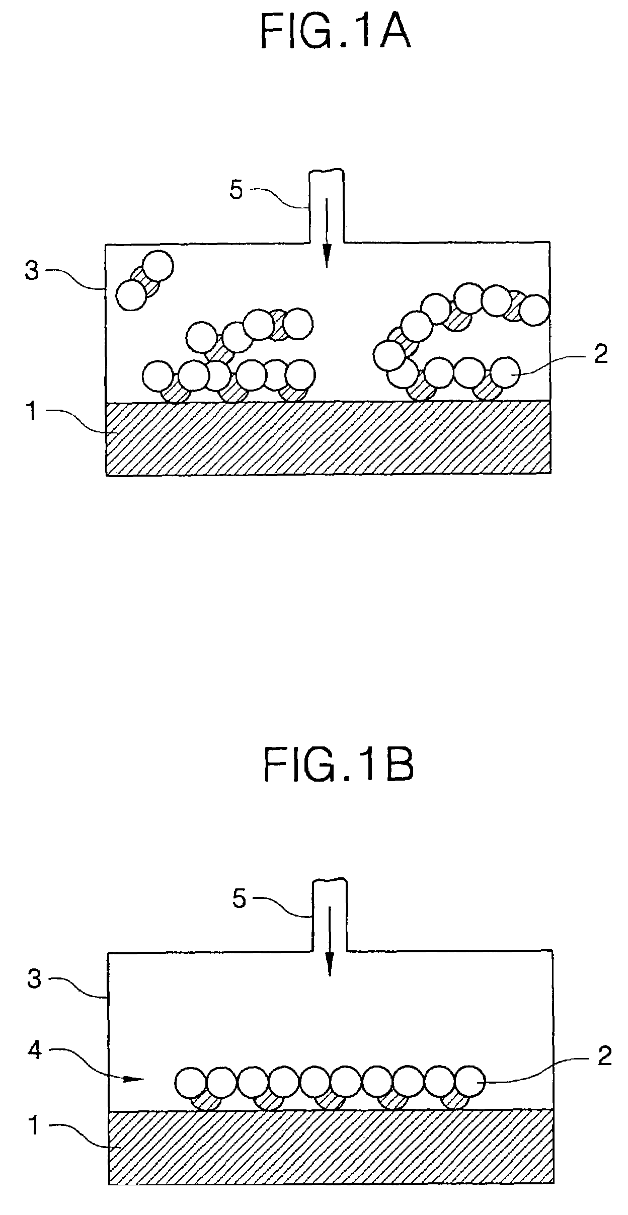
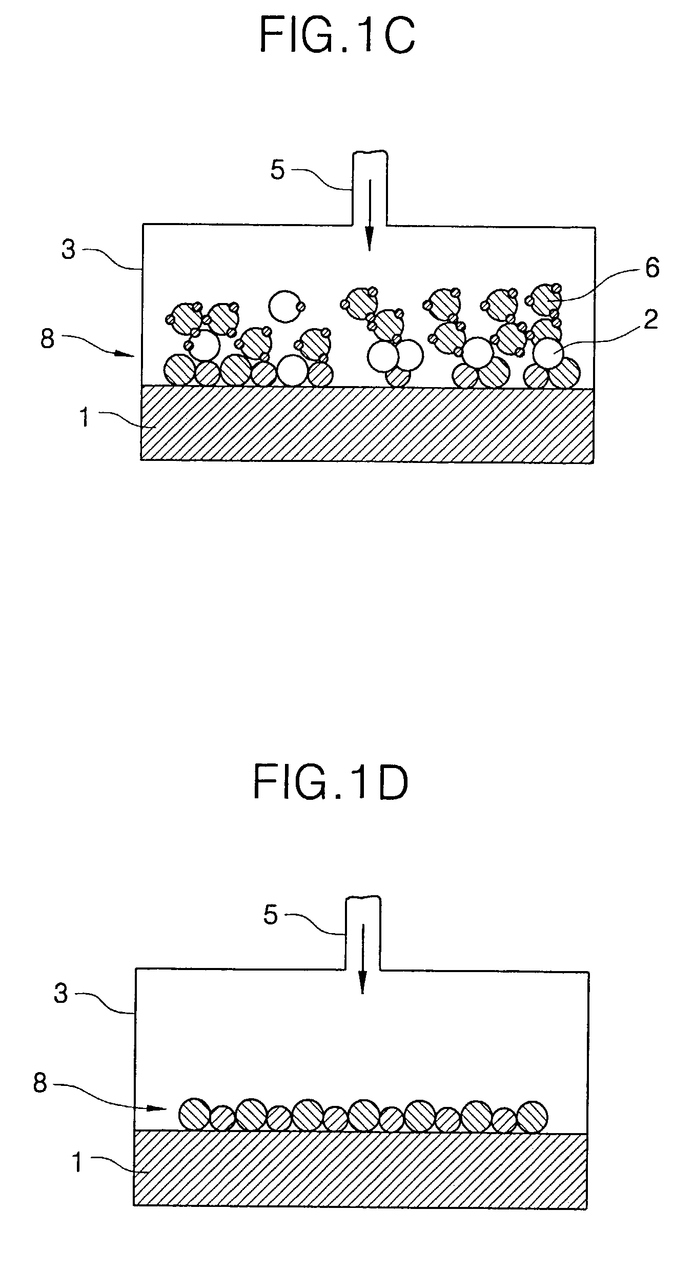
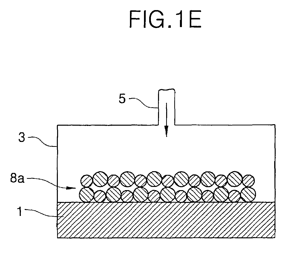
[0024]The present invention now will be described more fully hereinafter with reference to the accompanying drawings, in which embodiments of the invention are shown. However, this invention should not be construed as limited to the embodiments set forth herein. Rather, these embodiments are provided so that this disclosure will be thorough and complete, and will fully convey the scope of the invention to those skilled in the art. In the drawings, the thickness of layers and regions are exaggerated for clarity. Like numbers refer to like elements throughout. It will be understood that when an element such as a layer, region or substrate is referred to as being “on” or extending “onto” another element, it can be directly on or extend directly onto the other element or intervening elements may also be present. In contrast, when an element is referred to as being “directly on” or extending “directly onto” another element, there are no intervening elements present. Also, each embodiment...


PUM

PropertyMeasurementUnit
pressureaaaaaaaaaa
temperatureaaaaaaaaaa

Abstract

A thin film is formed using an atomic layer deposition process, by introducing a first reacting material including tantalum precursors and titanium precursors onto a substrate. A portion of the first reacting material is chemisorbed onto the substrate. Then, a second reacting material including oxygen is introduced onto the substrate. A portion of the second reacting material is also chemisorbed onto the substrate, to form an atomic layer of a solid material on the substrate. The solid material may be used as a dielectric layer of the capacitor and/or a gate dielectric layer of the transistor.

Description

RELATED APPLICATION[0001]This application claims the benefit of Korean Patent Application No. 2002-44318, filed Jul. 26, 2002, the disclosure of which is hereby incorporated herein by reference in its entirety as if set forth fully herein.FIELD OF THE INVENTION[0002]The present invention relates to methods of forming thin films, and more particularly to methods of forming thin films through Atomic Layer Deposition (ALD).BACKGROUND OF THE INVENTION[0003]Integrated circuit devices, such as logic and memory devices, are widely used in consumer and commercial applications. As the integration density of integrated circuit devices continues to increase, it may be desirable to form ultra thin layers, such as ultra thin dielectric layers, on a semiconductor substrate. These dielectric layers may be used, for example, as a gate dielectric layer of an insulated gate field effect transistor, also referred to as a MOSFET, and / or as a capacitor dielectric for an integrated circuit capacitor. As ...

Claims


Application Information

Patent Timeline
Patent Type & Authority Patents(United States)
IPC IPC(8): C23C16/40C23C16/44H01L21/205C23C16/455H01L21/02H01L21/316
CPCC23C16/405C23C16/45531C23C16/45542C23C16/45553H01L21/31604H01L21/31683H01L28/90H01L21/02277H01L21/02205H01L21/0228H01L21/02194H01L21/02274H01L21/205H01L21/02348H01L21/02337
Inventor PARK, IN-SUNGCHUNG, JEONG-HEEYEO, JAE-HYUN
Owner SAMSUNG ELECTRONICS CO LTD
Why Eureka
Try Eureka