MIM structure and fabrication process with improved capacitance reliability

a technology of capacitance reliability and fabrication process, which is applied in the direction of capacitors, instruments, semiconductor devices, etc., can solve the problems of increased power consumption, reduced power supply to circuitry, and increased power consumption, so as to reduce interdiffusion and improve capacitance reliability

Inactive Publication Date: 2007-04-17
TAIWAN SEMICON MFG CO LTD
View PDF4 Cites 4 Cited by
  • Summary
  • Abstract
  • Description
  • Claims
  • Application Information

AI Technical Summary

Benefits of technology

[0009]To achieve the foregoing and other objects, and in accordance with the purposes of the present invention, as embodied and broadly described herein, the present invention provides an MIM structure and method for forming the same with improved capacitance reliability by reducing interdiffusion of an MIM electrode and capacitive dielectric.

Problems solved by technology

One immediate problem with the integration of analog and digital circuitry blocks is the increase in power consumption.
The design constraints that inform the design of digital blocks include the need for fast signal transmission and low power consumption.
On the other hand in analog circuitry, as device sizes have decreased, the power supply to the circuitry has been decreased, leading to susceptibility of a signal to noise levels in the circuitry.
Electronic mismatch of circuitry components results in reduced signal processing quality and is adversely affected by deviations in processing conditions or the physical stability of component structures in processing and operating environments, for example a capacitance value of an MIM structure.
The capacitance of an MIM capacitor structure may be affected by several variables including the thickness of the capacitive dielectric layer which may be adversely affected by processing and operating conditions.

Method used


Image

  • MIM structure and fabrication process with improved capacitance reliability
  • MIM structure and fabrication process with improved capacitance reliability
  • MIM structure and fabrication process with improved capacitance reliability

Examples


Embodiment Construction

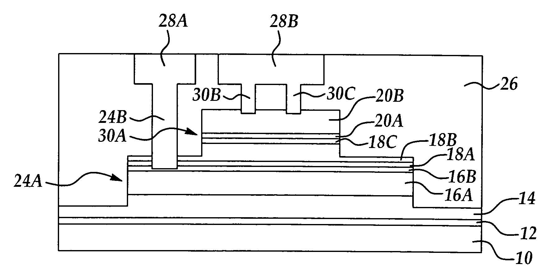
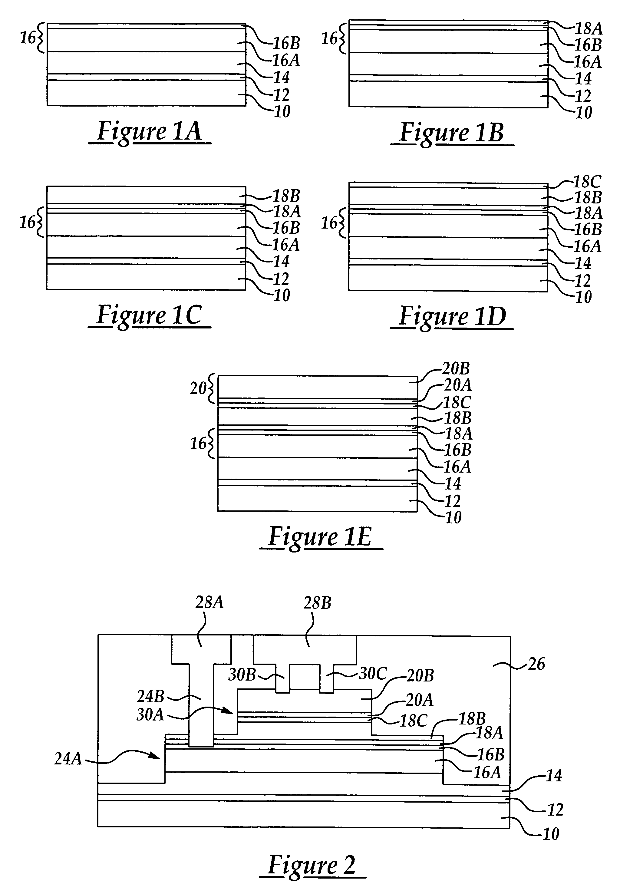
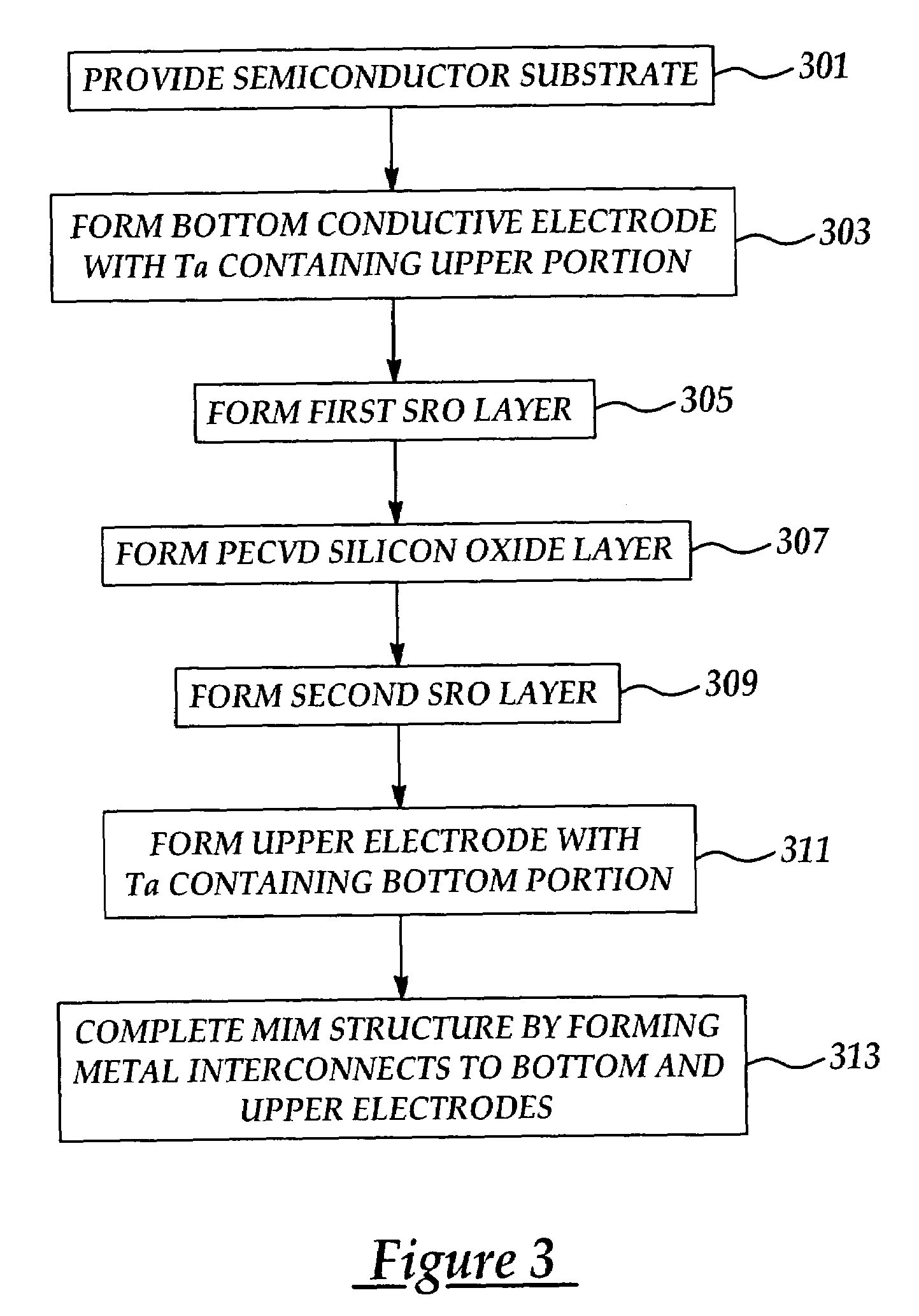
[0015]The method and MIM capacitor structure according to the present invention is more clearly described by referring to FIGS. 1A–1E where cross sectional views at stages of manufacture are shown in forming an MIM capacitor structure.

[0016]FIG. 1A shows by way of example, an embodiment of the present invention in forming an exemplary MIM structure. For example referring to FIG. 1A is shown a semiconductor substrate 10, for example silicon, having a layer of silicon nitride 12 deposited thereover by conventional methods, for example LPCVD to a thickness of about 400 to about 800 Angstroms. An undoped silicate glass (USG) layer 14 is then deposited by conventional CVD methods to a thickness of about 1000 Angstroms. A bottom conductive electrode (plate) 16 is then deposited by conventional means. Preferably, the bottom electrode 16 if formed of at least one conductive layer, for example including any conductive metal, more preferably aluminum-copper (AlCu) alloy, tantalum (Ta), titani...


PUM

PropertyMeasurementUnit
thicknessaaaaaaaaaa
thicknessaaaaaaaaaa
thicknessaaaaaaaaaa

Abstract

An MIM structure and method for forming the same the method including forming a bottom conductive electrode overlying a semiconducting substrate; forming a first protection layer on the conductive electrode; forming a dielectric layer on the first protection layer; and, forming an upper conductive electrode on the dielectric layer to form a metal-insulator-metal (MIM) structure.

Description

FIELD OF THE INVENTION[0001]This invention generally relates to metal-insulator-metal structures and more particularly to an MIM structure and method for depositing plasma enhanced oxide to achieve a MIM capacitor structure with improved capacitance reliability.BACKGROUND OF THE INVENTION[0002]Advances in technology have resulted in an increasing demand for system-on-chip products where both analog and digital signal processing are desirable. For example analog circuits capture an analog signal from the surrounding environment and transform the signal into bits which are then transformed into signals for driving digital circuitry and output functions. Increasingly it is advantageous to have both the analog circuitry and digital circuitry in close proximity, for example in the form digital blocks and analog blocks of circuitry which function together to implement the function of the system, also referred to as mixed mode systems.[0003]One immediate problem with the integration of ana...

Claims


Application Information

Patent Timeline
Patent Type & Authority Patents(United States)
IPC IPC(8): H01L29/00G02F1/1337
CPCH01L28/40Y10S438/957
Inventor LIAO, MIAO-CHENGCHENG, KUO-HSIENLIN, CHENG-CHAOHSU, SHAO-TAWANG, YING-LANG
Owner TAIWAN SEMICON MFG CO LTD
Why Eureka
Try Eureka