Optical switching element, and device, optically addressed type display medium and display each using the optical switching element

a technology of optical switching element and optical address, which is applied in the direction of electrographic process apparatus, instruments, corona discharge, etc., can solve the problems of low ctm content layer (a ctm-poor layer), uneven ctm concentration distribution, and drift of applied voltage, so as to achieve the effect of suppressing asymmetry of electrical characteristics more effectively

Inactive Publication Date: 2007-04-17
FUJIFILM BUSINESS INNOVATION CORP
View PDF9 Cites 1 Cited by
  • Summary
  • Abstract
  • Description
  • Claims
  • Application Information

AI Technical Summary

Benefits of technology

[0027]In a more preferred manner, the first charge generating layer and the second charge generating each absorb substantially the same quantity of light, so that asymmetry of the electrical characteristics can be suppressed more effectively.

Problems solved by technology

As a result of analysis, however, it has been found that in a conventional charge transporting layer (CTL) comprising an charge transporting material (CTM) and a binder polymer in a ratio of 40:60, the CTM concentration is unevenly distributed in the thickness direction of the CTL and that there is a low CTM content layer (a CTM-poor layer) particularly in the vicinity of the surface of the known CTL.
This can cause the following problems.
Such a state can accumulate in the display layer causing a drift of the applied voltage and a degradation in the display characteristics.
Moreover, the thickness of the CTM-poor layer increases with that of the CTL.
Therefore, if the CTL is thick, the degree of the asymmetry can be high and the degradation in the display characteristics can be significant.
Therefore, there are difficulties in increasing the thickness of the CTL, and the design of the balance with the impedance of the display layer is restricted.
Thus, the OPC element cannot offer sufficient driving performance; the display characteristics are degraded; and the driving voltage margin is narrow.

Method used


Image

  • Optical switching element, and device, optically addressed type display medium and display each using the optical switching element
  • Optical switching element, and device, optically addressed type display medium and display each using the optical switching element
  • Optical switching element, and device, optically addressed type display medium and display each using the optical switching element

Examples


example 1

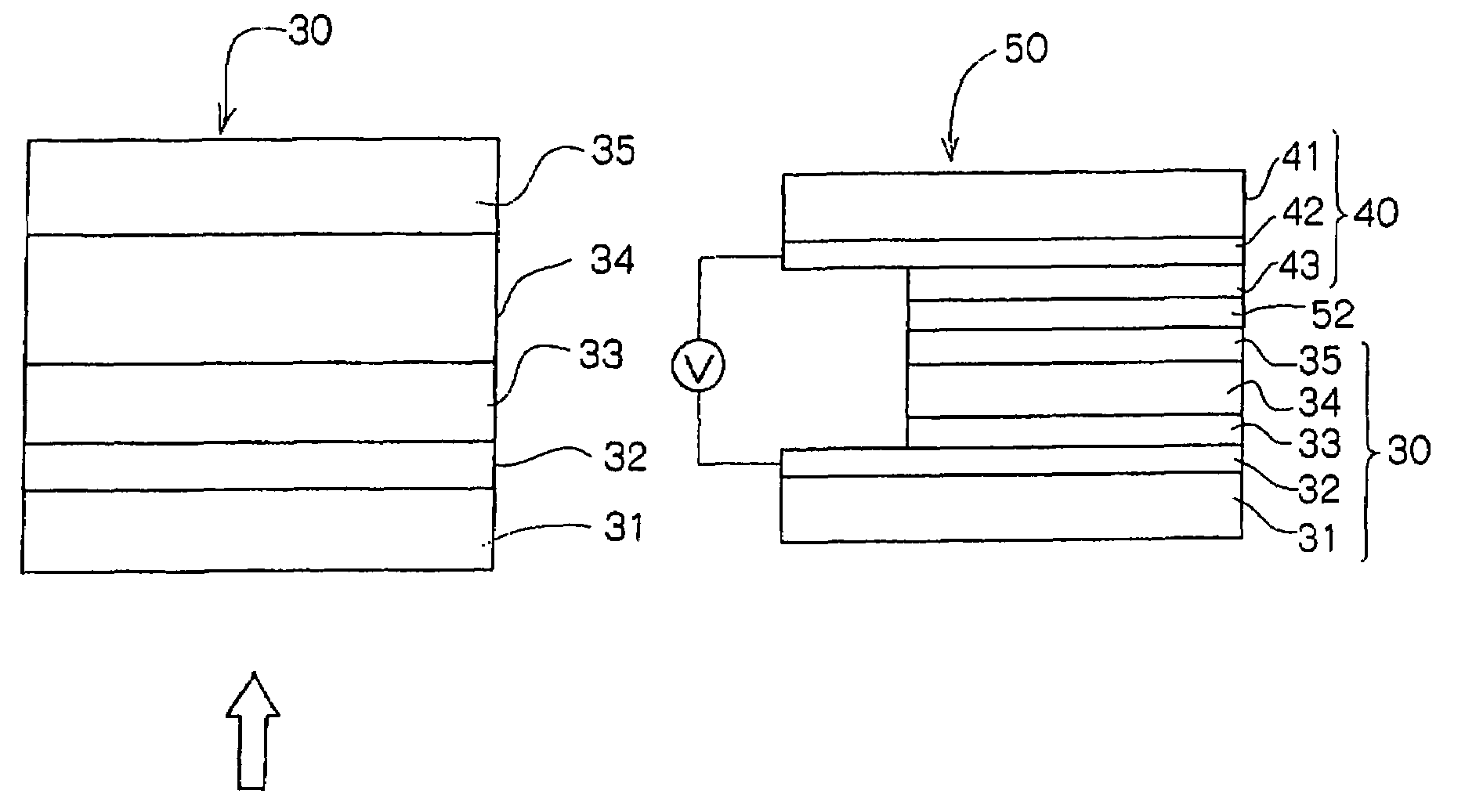
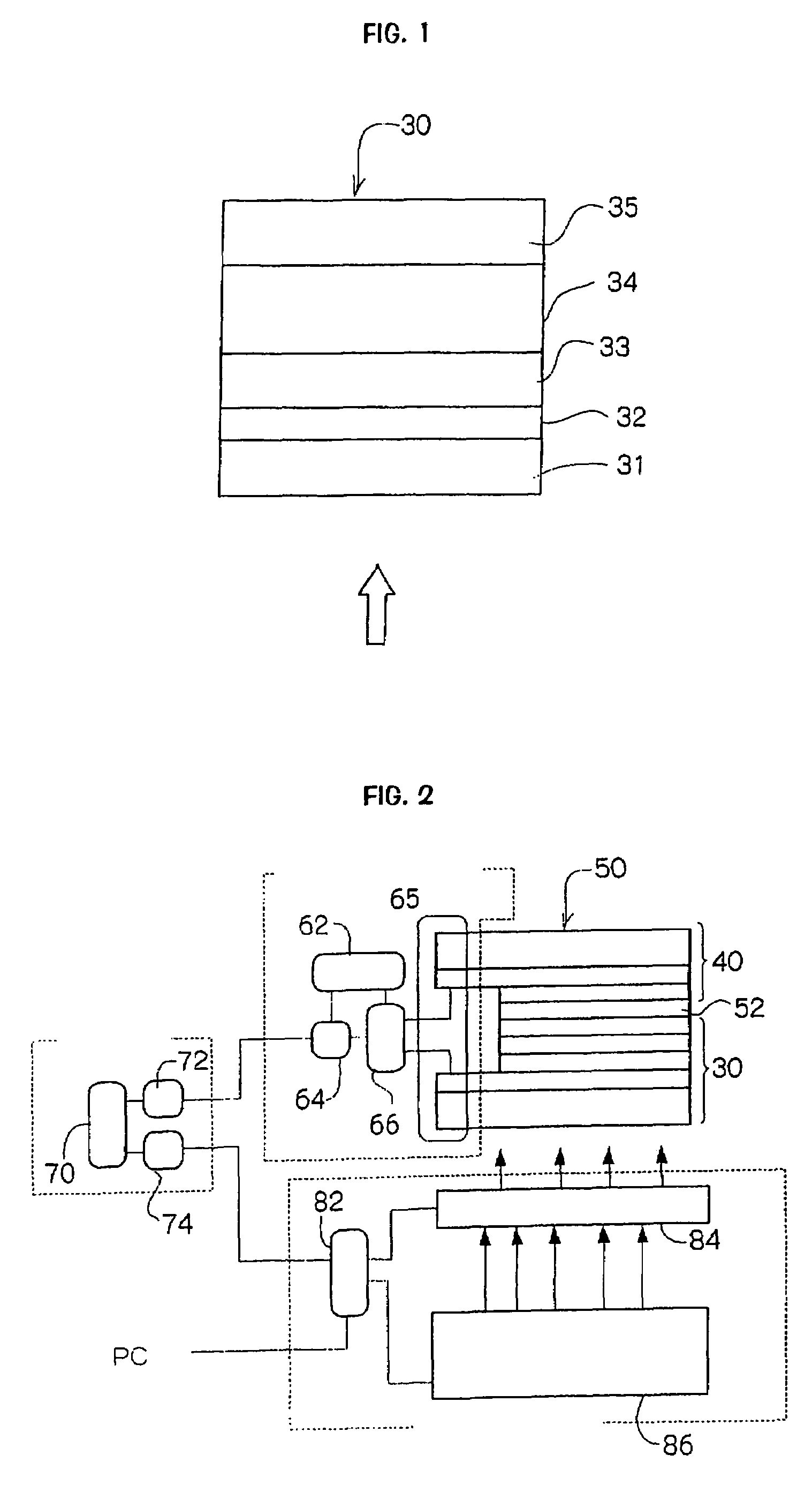
[0114]An optically addressed type display medium having the same structure as shown in FIG. 2 is prepared by the process as shown below.

[0115]The lower charge generating layer 33 is formed on an ITO film (800 Å in thickness), which is formed as the electrode layer 32 on a polyethylene terephthalate (PET) substrate 31 (125 μm in thickness). Specifically, the charge generating material used is hydroxygallium phthalocyanine with an ionization potential of 5.31 eV (having strong diffraction peaks in X-ray diffraction spectrum at Bragg angles (2θ±0.2°) of 7.0°, 7.5°, 10.5°, 11.7°, 12.7°, 17.3°, 18.1°, 24.5°, 26.2°, and 27.1°), and the binder resin used is polyvinyl butyral. The charge generating material and the binder resin are mixed in a weight ratio of 1:1 and dispersed in butanol to form a 2% by weight dispersion (Coating Liquid A). The dispersion is applied to the substrate by spin coating and dried to form the charge generating layer 33. The resulting charge generating layer 33 has...

example 2

[0136]Display media (C-1 and C-2) are produced according to the process of Example 1, except that some steps are modified as shown below.

Display Medium C-1 (Example of the Invention)

[0137]The lower charge generating layer 33 is formed as shown below. The charge generating material used is hydroxygallium phthalocyanine with an ionization potential of 5.31 eV (having strong diffraction peaks in X-ray diffraction spectrum at Bragg angles (2θ±0.2°) of 7.0°, 7.5°, 10.5°, 11.7°, 12.7°, 17.3°, 18.1°, 24.5°, 26.2°, and 27.1°), and the binder resin used is polyvinyl butyral. The charge generating material and the binder resin are mixed in a weight ratio of 1:1 and dispersed in butanol to form a 2% by weight dispersion (Coating Liquid C). The dispersion is applied to the substrate by spin coating and dried to form the charge generating layer 33. The resulting charge generating layer 33 has a light absorptance of 45%.

[0138]The charge transporting layer 34 is then formed as shown below A charge...

example 3

[0146]A display medium (D-1) is produced according to the process of Example 1, except that some steps are modified as shown below.

Display Medium D-1 (Example of the Invention)

[0147]The charge transporting layer 34 is formed as shown below. The charge transporting material used is a charge transporting polymer (Illustrative Compound (58)) synthesized by the process as shown below. The charge transporting polymer is dissolved in monochlorobenzene to form a 10% by weight solution. The solution is applied using an applicator (Gap: 100 μm) and dried to form the charge transporting layer 34 with a thickness of 7 μm on the lower charge generating layer 33.

Synthesis of Charge Transporting Polymer (Illustrative Compound (58))

[0148]To a 50 ml flask are added 2.0 g of 3,3′-dimethyl-N,N′-bis(3,4-dimethylphenyl)-N,N′-bis[4-(2-methoxycarbonylethyl)phenyl]-[1,1′-biphenyl]-4,4′-diamine, 4.0 g of ethylene glycol and 0.1 g of tetrabutoxytitanium and heated and refluxed under a stream of nitrogen for...


PUM

PropertyMeasurementUnit
thickaaaaaaaaaa
thickaaaaaaaaaa
Bragg anglesaaaaaaaaaa

Abstract

The invention provides an optical switching element and a device, an optically addressed type display medium and a display each including such an optical switching element. The optical switching element comprising an optical switching layer including lower and upper charge generating layers and a charge transporting layer sandwiched therebetween, wherein the optical switching element has at least one of the following characteristics. (1) In the charge transporting layer, a charge transporting material to binder polymer ratio calculated according to the formula: [charge transporting material/(charge transporting material+binder polymer)]×100 (% by weight) is 50% by weight or more; (2) a polymer compound is used as the charge transporting material; and (3) the charge generating layer on the light incident side (the lower charge generating layer) has a lower light absorptance than that of the other charge generating layer (the upper charge generating layer).

Description

CROSS-REFERENCE TO RELATED APPLICATIONS[0001]This application claims benefit of and priority to Japanese Patent Application No. 2003-182813, filed on Jun. 26, 2003, which is incorporated herein by reference in its entirety for all purposes.BACKGROUND OF THE INVENTION[0002]1. Field of the Invention[0003]The present invention relates to an optical switching element and to a device, an optically addressed type display medium and a display that are the optical switching element.[0004]2. Description of the Related Art[0005]In recent years, optically addressed spatial modulating devices, in which a photoconductive switching element and a display element are combined, have been developed. Such devices are being utilized as light bulbs for projectors or the like and are being investigated for potential uses in the field of optical information processing as disclosed in “Liquid Crystal Spatial Modulators and Information Processing”, (Liquid Crystal), Vol. 2, No. 1, 1998, pp. 3–18.[0006]In th...

Claims


Application Information

Patent Timeline
Patent Type & Authority Patents(United States)
IPC IPC(8): G02F1/15G02F1/133G02F1/135
CPCG02F1/1354
Inventor HIKICHI, TAKEHITOKOBAYASHI, HIDEO
Owner FUJIFILM BUSINESS INNOVATION CORP
Why Eureka
Try Eureka