Decode circuitry and a display device using the same

a display device and circuit technology, applied in the field of decoding circuits, can solve the problems of affecting the size reduction of the display device, increasing the current consumption of the circuit, and the inability to transmit reference voltage at a fully accurate level, etc., and achieve the effect of fast decoding operation

Inactive Publication Date: 2007-04-24
MITSUBISHI ELECTRIC CORP
View PDF7 Cites 15 Cited by
  • Summary
  • Abstract
  • Description
  • Claims
  • Application Information

AI Technical Summary

Benefits of technology

[0021]An object of the invention is to provide a reliable decode circuit that occupies a small layout area, and can perform a fast decode operation to produce an output signal according to an input signal.
[0022]Another object of the invention is provide a reliable decode circuit for digital-to-analog conversion that can implement a fast decoding of input data to produce an analog signal with a reduced number of elements, as well as an image display device including such decode circuit.
[0027]A second sub-decode circuit formed of one serial signal transmission path is arranged for each of the plurality of first sub-decode circuits. Therefore, the switching elements connected to the output line can be reduced in number, and the parasitic capacitance of the output line can be reduced so that a decode result signal can be produced fast. Since only one serial signal transmission path is arranged for each of the plurality of first sub-decode circuits, components of the decode circuit of the invention can be reduced in number, and accordingly, the layout area can be reduced.
[0028]Since the switching elements are reduced in number, a drive load on a buffer circuit producing control signals for driving the switching elements is reduced, and the driving power of the buffer circuit can be reduced. Accordingly, the power consumption and the layout area of the buffer circuit can be reduced.
[0029]Since the parasitic capacitance of the output signal line is reduced, it is possible to reduce the driving power of the buffer circuit driving the electric signal transmitted to the output signal line, and the power consumption of this buffer circuit can be reduced. Since it is possible to reduce the driving power of the transistors which are components of the buffer circuit, it is possible to reduce the sizes (channel widths) of the transistors, and accordingly, the low power consumption and the small layout area can be achieved.
[0030]Further, in the display device, the occupation area of the digital-to-analog converter circuit is reduced, and thereby the area of an entire of the display device is reduced.

Problems solved by technology

Therefore, where a drive circuit is formed to be integrated with a display panel on the same chip, the chip real estate is greatly increased, which significantly impairs reduction in size of the display device.
This causes a problem of increase in current consumption of a circuit producing a control signal (select signal) corresponding to input pixel data.
Therefore, when the change timing of the reference voltage deviates from the timing of the select timing signal resulting from the lower bit decoding, such a problem occurs that the reference voltage at a fully accurate level cannot be transmitted.
Each reference current must be changed one quantum step at a time over the gradation levels which correspond in number to the lower bits, and this complicates the construction of the reference voltage generating unit.
This results in a problem that the elements in the gradation select unit are large in number, and the circuit layout area is large.
Thus, such a period of time is present that the parasitic capacitance of the output line is increased to cause a problem that the gradation level on the output line cannot be updated fast according to the input pixel data.
This extremely restricts the degree of freedom in layout, to cause a problem that the efficient circuit design is difficult to achieve.
In the case where the P- or N-channel MOS transistor is used as the switching element for the gradation selection and the amplitude of the control signal is increased, dielectric-breakdown voltage characteristics deteriorate, and the element durability is adversely affected.
As a countermeasure, an analog switch of a CMOS type may be simply used for the switching element, a greater load capacitance (on-capacitance) comes to be parasitic on the output line, and it becomes impossible to perform a fast decode operation.
Further, the total number of switching elements is great, and it becomes difficult to perform an efficient layout within a small area, and yield lowers in product manufacturing.
The construction of the decode circuit described above can be applied to the circuits other than the digital-to-analog converter circuit for producing the analog voltage according to the input digital data, and it can be applied, e.g., to a switch matrix circuit establishing a transmission path of a certain signal by a decode circuit, and in such a case, similar problems would occur.

Method used


Image

  • Decode circuitry and a display device using the same
  • Decode circuitry and a display device using the same
  • Decode circuitry and a display device using the same

Examples


first embodiment

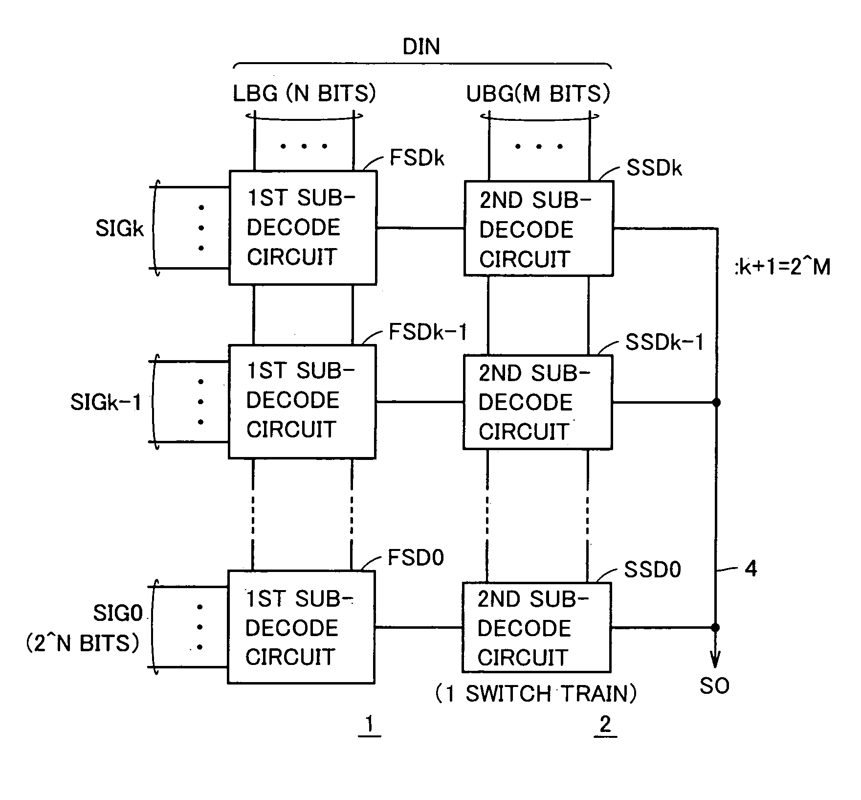
[0044]FIG. 1 schematically shows a construction of a decode circuit according to a first embodiment of the invention. In FIG. 1, the decode circuit includes a first decode circuit 1 for selecting one candidate from each of selection candidate groups SIG0–SIGk according to a lower bit group LBG of multi-bit data DIN, and a second decode circuit 2 for producing an output signal SO by selecting one output from the outputs of first decode circuit 1 according to an upper bit group UBG of multi-bit data DIN.

[0045]In multi-bit data DIN, lower bit group LBG includes N bits, and upper bit group UBG includes M bits. Each of selection candidate groups SIG0–SIGk includes an electric signal of 2^N bits. The electric signal is any of a logic signal, a voltage and a current. These selection candidate groups SIG0–SIGk are divided into groups according to a bit number M of upper bit group UBG, and satisfy a relationship of k+1=2^M.

[0046]The first decode circuit 1 includes first sub-decode circuits F...

second embodiment

[0104]FIG. 7 shows a construction of a decode circuit according to a second embodiment of the invention. The decode circuit shown in FIG. 7 employs four-bit data D3–D0, for selecting one from 16 reference voltages V0–V15. This decode circuit may be utilized for the decode circuit of the digital-to-analog conversion unit in the image display device implementing the 16-level gradation display. Most significant bit MSB is bit D3, and least significant bit LSB is bit D0. The decode operation is first performed according to upper bits D3 and D2, and subsequently the final decode operation is performed according to the lower bit group.

[0105]Since data bits D3–D0 represent the numbers indicating reference voltages V0–V15, the selection candidate reference voltages V0–V15 are divided into reference voltage sets of V(4n), V(4n+1), V(4n+2) and V(4n+3), where n is an integer from 0 to 3. First sub-decode circuit FSD0 is arranged for the set of reference voltages V(4n: n=0, 1, 2, 3), first sub-...

third embodiment

[0119]FIG. 9 schematically shows a construction of a display device according to a third embodiment of the invention. In FIG. 9, the display device includes a pixel array (display panel) 20 having pixels PX arranged in rows and columns. In the pixel array 20, gate lines G0–Gm are arranged corresponding to the respective rows of pixels PX, and data lines DL are arranged corresponding to the respective columns of pixels PX. FIG. 9 representatively shows pixels PX connected to gate line G0 in pixel array 20. Data lines DL are divided into groups each including the data lines of k in number. This is because the decode operation (digital-to-analog converting operation) is effected in units of sets or groups of the data lines as will be described later.

[0120]A vertical drive circuit 21 sequentially drives gate lines G0–Gm to the selected state every horizontal scanning period. Vertical drive circuit 21 receives a vertical operation start instruction signal VST and a vertical shift clock s...


PUM


Abstract

Multi-bit input data is divided into at least a first bit group and a second bit group, and each of first sub-decode circuits selects one selection target signal / voltage from selection target signal / voltage group in accordance with the first bit group. Then, one signal / voltage is selected according to the second bit group from the signals / voltages selected by the first sub-decode circuits, and is transmitted to an output signal line. Each of second sub-decode circuits is formed of a single train of series switches, and only one of the switch train is made conductive to transmit a finally selected signal / voltage to the output signal line.

Description

BACKGROUND OF THE INVENTION[0001]1. Field of the Invention[0002]The present invention relates to a decode circuit for decoding a multi-bit digital signal to produce an electric signal (voltage) corresponding to the multi-bit digital signal, and particularly to a decode circuit used in digital-to-analog conversion of converting the multi-bit digital signal to an analog signal, as well as to a display device supporting the decode circuit. More specifically, the invention relates to a configuration of a decode circuit in a digital-to-analog converter producing a pixel write voltage corresponding to input pixel data in an image display unit.[0003]2. Description of the Background Art[0004]For selecting one output candidate from a plurality of output candidates, a decode circuit is generally utilized. By utilizing a digital signal of n bits, one candidate can be selected from possible outputs of the n-th power of 2 in number, and a circuit layout area can be reduced, as compared with a co...

Claims


Application Information

Patent Timeline
Patent Type & Authority Patents(United States)
IPC IPC(8): H03M5/02
CPCH03M1/682H03M7/04H03M1/765H03M1/66G02F1/133G09G3/20
Inventor HASHIDO, RYUICHIMURAI, HIROYUKI
Owner MITSUBISHI ELECTRIC CORP
Why Eureka
Try Eureka