Low cost fabrication of high resistivity resistors

a technology of resistors and resistors, which is applied in the fabrication of bicmos, bicmos or silicongermanium bicmos semiconductor devices, and can solve the problems of increasing the complexity of the bipolar complementary metal oxide semiconductor (“bicmos”) process and affecting the fabrication of other devices, so as to improve the thermal stability of the circuit, improve the resistance, and reduce the cost

Inactive Publication Date: 2007-05-15
NEWPORT FAB
View PDF4 Cites 2 Cited by
  • Summary
  • Abstract
  • Description
  • Claims
  • Application Information

AI Technical Summary

Benefits of technology

[0012]The resistor illustrated in FIG. 1 has a relatively low resistivity of approximately 100 ohms per square, as pointed out above. There are certain advantages to fabricating a resistor with a higher resistivity, for example, temperature coefficient of the resistor, also referred to as “TCR”, can be improved. Simply stated, TCR expresses the change in resistance per degree C. from the resistance value a

Problems solved by technology

A bipolar complementary metal oxide semiconductor (“BiCMOS”) process increases the complexity by adding the concurrent fabrication of bipolar devices—for example, conventional NPN or PN

Method used


Image

  • Low cost fabrication of high resistivity resistors
  • Low cost fabrication of high resistivity resistors
  • Low cost fabrication of high resistivity resistors

Examples


Embodiment Construction

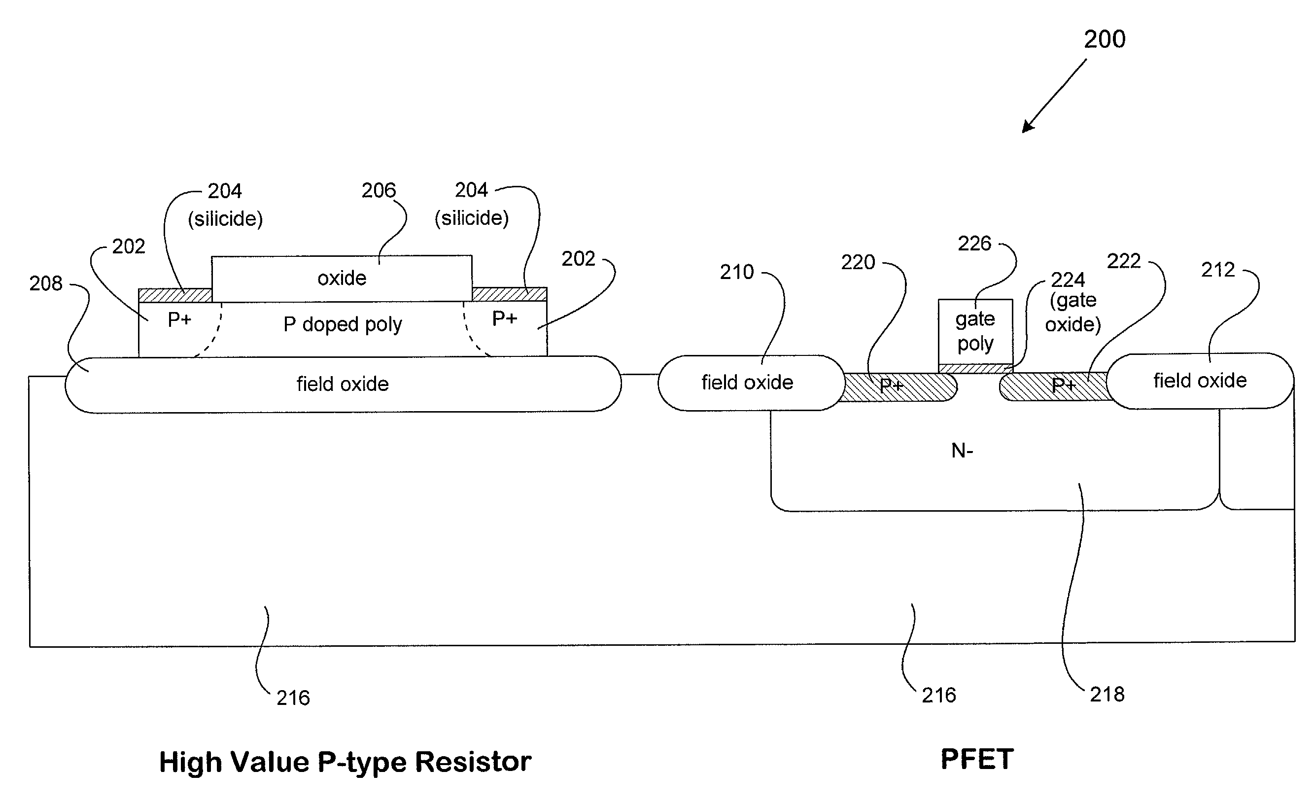
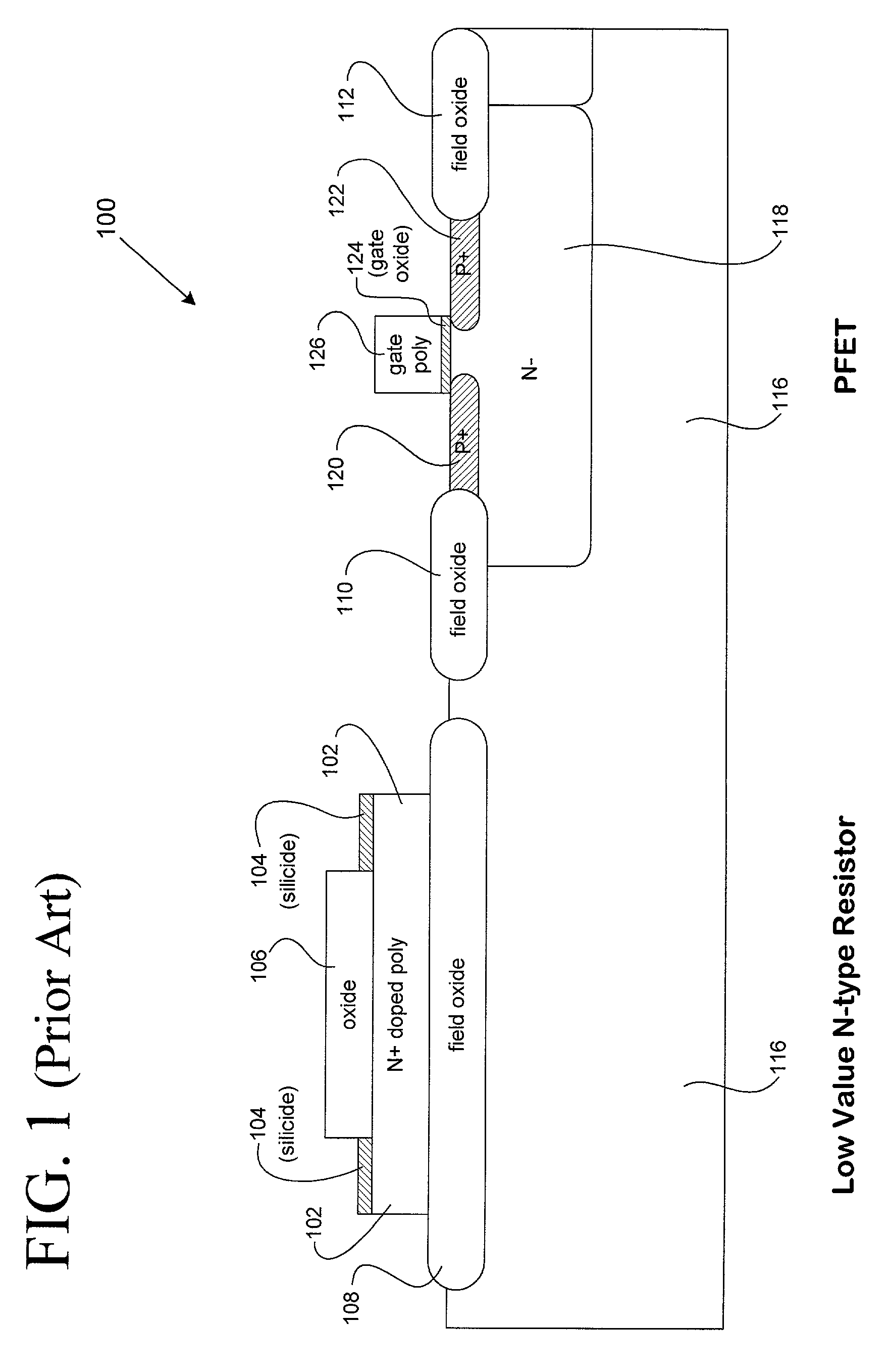
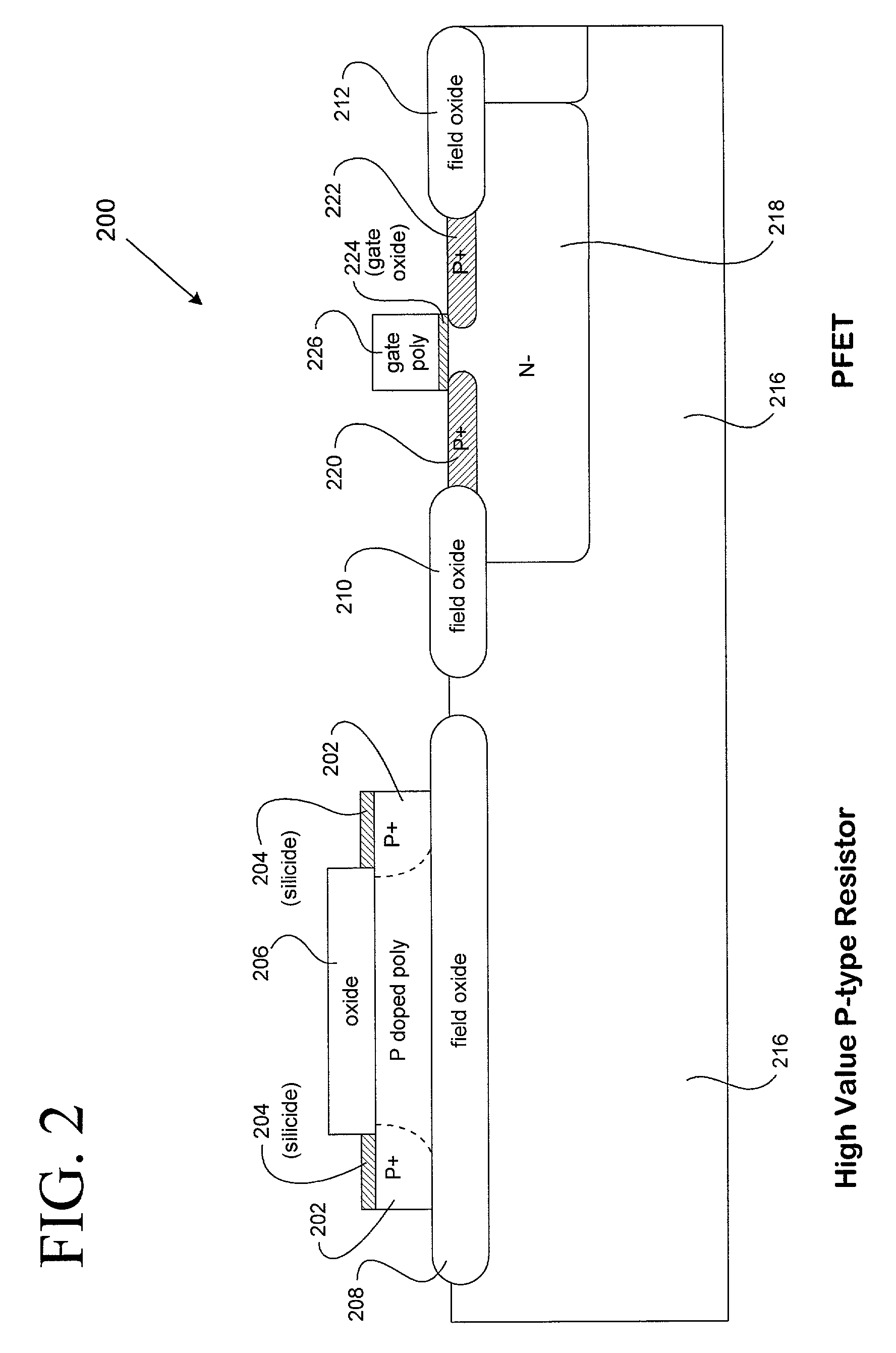
[0019]The present invention is directed to low cost fabrication of high resistivity resistors. The following description contains specific information pertaining to the implementation of the present invention. One skilled in the art will recognize that the present invention may be implemented in a manner different from that specifically discussed in the present application. Moreover, some of the specific details of the invention are not discussed in order to not obscure the invention. The specific details not described in the present application are within the knowledge of a person of ordinary skill in the art.

[0020]The drawings in the present application and their accompanying detailed description are directed to merely example embodiments of the invention. To maintain brevity, other embodiments of the invention which use the principles of the present invention are not specifically described in the present application and are not specifically illustrated by the present drawings.

[00...


PUM


Abstract

In one disclosed embodiment a layer is formed over a transistor gate and a field oxide region. For example, a polycrystalline silicon layer can be deposited over a PFET gate oxide and a silicon dioxide isolation region on the same chip. The layer is then doped over the transistor gate without doping the layer over the field oxide. A photoresist layer can be used as a barrier to implant doping, for example, to block N+ doping over the field oxide region. The entire layer is then doped, for example, with P type dopant after removal of the doping barrier. The second doping results in formation of a high resistivity resistor over the field oxide region, without affecting the transistor gate. Contact regions are then formed of a silicide, for example, for connecting the resistor to other devices.

Description

BACKGROUND OF THE INVENTION[0001]1. Field of the Invention[0002]The present invention relates to the field of fabrication of semiconductor devices. More specifically, the invention relates to the fabrication of CMOS, BiCMOS, or silicon-germanium BiCMOS semiconductor devices.[0003]2. Related Art[0004]In the manufacture of large scale integration semiconductor devices, several types of devices are fabricated concurrently on the same chip or wafer. For example, in a complementary metal oxide semiconductor (“CMOS”) process both P-channel field effect transistors (“PFET”) and N-channel field effect transistors (“NFET”) are manufactured on the same chip concurrently. A bipolar complementary metal oxide semiconductor (“BiCMOS”) process increases the complexity by adding the concurrent fabrication of bipolar devices—for example, conventional NPN or PNP transistors—to the same chip. By growing a thin silicon-germanium layer as the base of a bipolar transistor on a silicon wafer, a heterojunc...

Claims


Application Information

Patent Timeline
IPC IPC(8): H01L21/8234H01L21/02H01L27/06H01L27/12
CPCH01L27/0629H01L27/1203H01L28/20
Inventor RACANELLI, MARCO
Owner NEWPORT FAB
Why Eureka
Try Eureka