
Multilayer transfer patterning using polymer-on-polymer stamping

a technology of polymer-on-polymer and transfer patterning, which is applied in the field of multi-layer transfer patterning using polymer-on-polymer stamping, can solve the problems of increasing manufacturing costs, limiting the application range of light-based lithography to curved, non-planar surfaces,

Inactive Publication Date: 2007-05-22
MASSACHUSETTS INST OF TECH
View PDF6 Cites 13 Cited by
  • Summary
  • Abstract
  • Description
  • Claims
  • Application Information

AI Technical Summary

Benefits of technology

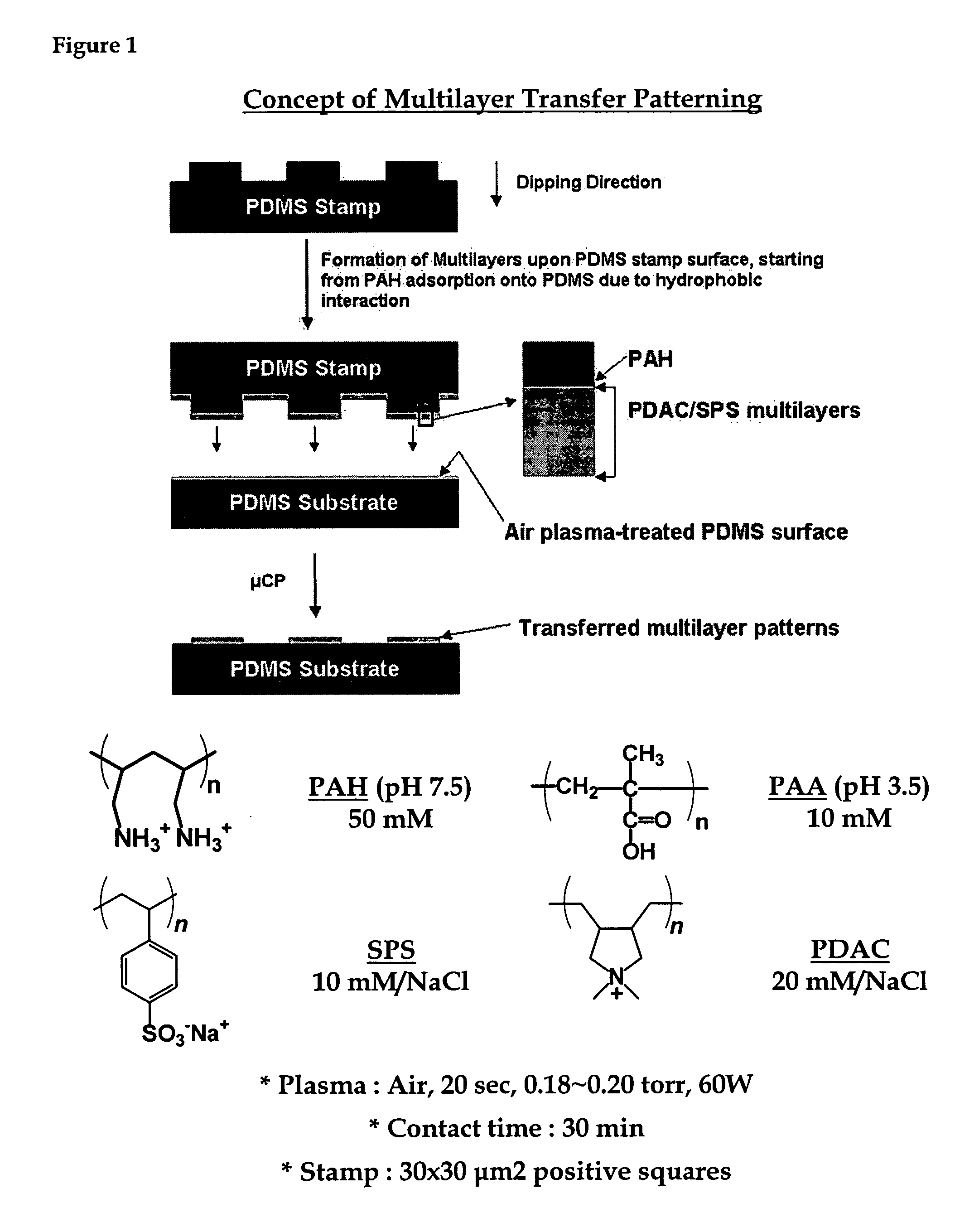
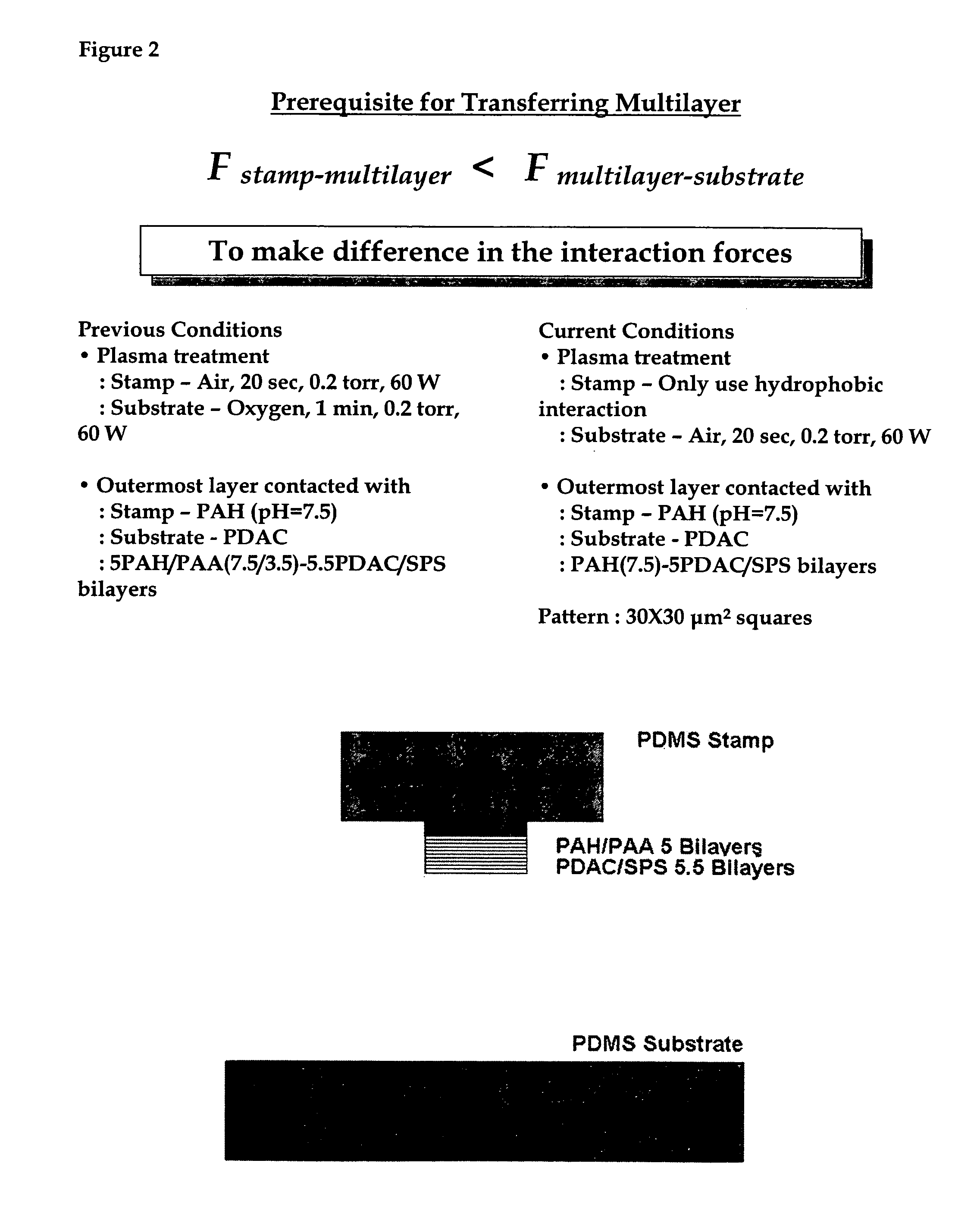
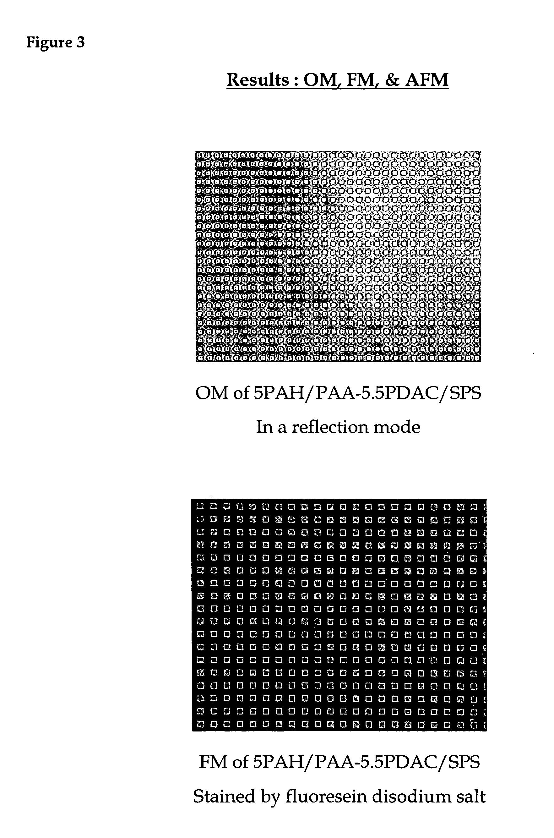
[0009]One aspect of the present invention relates to a method of transferring a patterned polyelectrolyte multilayer from a first surface, e.g., a PDMS stamp, to a second surface, e.g. fabric or a non-woven material. Another aspect of the present invention relates to a stamp comprising a surface coated with a polyelectrolyte multilayer suitable for transfer to a substrate using the aforementioned method of transferring patterned multilayers. In preferred embodiments, a layer-by-layer assembly process is used to prepare a multilayer on the first surface. In preferred embodiments, non-covalent interactions were employed to form multilayers on stamps with patterns. Fundamentally, the transfer of multilayer patterns from the first surface to the second surface was based on the difference in interaction forces between first surface and the multilayer; and the second surface and the multilayer. Patterned multilayers provided stable chemical functionalities, which can be used as reaction sites and as a means for incorporating other reagent molecules and particles. Multilayers containing chemicals or particles in their structures have also been transferred. The size and shape of patterns can be controlled by fabricating stamps with various kinds of patterns. The surface functionalities of transferred patterns can be controlled, e.g., by varying the polyelectrolytes from which the multilayers are formed.

Problems solved by technology

Finally, light-based lithography can be limited in its application to curved, nonplanar surfaces, such as optical lenses and fibers, and multiple processing steps are required to create three dimensional, multiple level microstructures.
Some challenges with this method include the need to tune the selectivity of deposition via processing conditions and polyion composition to achieve high selectivity.
Many of these methods require the design a photolytic component either within the film or in the underlying layers, and therefore limit the range of polymer films used in the approach, as well as increasing the cost of manufacturing.
Second, stamping atop continuous or patterned polymer thin films, followed by subsequent selective adsorption or deposition steps would generate complex multiple level heterostructures.

Method used


Image

  • Multilayer transfer patterning using polymer-on-polymer stamping
  • Multilayer transfer patterning using polymer-on-polymer stamping
  • Multilayer transfer patterning using polymer-on-polymer stamping

Examples


example 1

Stamping Copolymers on a Surface to Serve as Templates for Additional Layers

Materials

[0120]Poly(acrylic acid) sodium salt (MW=20,000) (PAA), sodium poly(styrene sulfonate) (MW=35,000) (SPS), and linear polyethyleneimine (MW=25,000) (LPEI) were obtained from Polysciences. Polydiallydimethyl ammonium chloride (MW=100,000–200,000) (PDAC) and branched polyethyleneimine (MW=25,000) (BPEI) were obtained from Aldrich. All polyelectrolytes were used as received without further purification. Polyelectrolyte dipping solutions were prepared with 18 MΩ Millipore water, and the pH of these solutions was adjusted with either HCl or NaOH. The concentrations of all polyelectrolytes were 0.01 M as based on the molecular repeat unit of the polymer, with the exception of the PDAC solution, which was 0.02M. Solutions were filtered with a 0.45 μm Acrodisc syringe filter (Pall Corporation) to remove any particulates. The copolymer of an oliogethylene oxide functionalized vinyl ether and maleic anhydride ...

example 2

Stamping Block Copolymer, Graft Copolymer and Polyelectrolytes—Stamping of PS-b-PAA Block Copolymer

Materials

[0125]Poly(diallyldimethylammonium chloride) (PDAC) of MW=150,000 was purchased from Aldrich. Sulfonated polystyrene (SPS) of MW=70,000 was obtained from Aldrich. Poly(allylamine hydrochloride) (PAH) of MW=50,000–65,000 and poly(acrylic acid) (PAA) with MW=90,000 were purchased from Aldrich; polystyrene-polyacrylic acid diblock copolymer (PS-b-PAA) with a PS block MW=66,500 and PAA block MW=4,500 was obtained from Polysource. The aminopropyltrimethoxy silane was also obtained from Aldrich. The stamp used to make prints on the multilayers was a PDMS stamp. It was made by pouring a commercial PDMS mix (Sylguard, 184 silicone elastomer kit) over a silicon master etched with the desired pattern.

Substrate Preparation

[0126]Three different substrates were used as platforms for the stamping of the PS-b-PAA block copolymer. Direct stamping onto polyelectrolyte multilayer substrates was...

example 3

Stamping of Polyelectrolytes on Charged Multilayer Surfaces

Substrate Preparation

[0129]The strong polyelectrolytes SPS and PDAC were used to form multilayer platforms on which solutions of the same polymers could be stamped. The platforms were built on glass slides cleaned with a dilute Lysol / water mixture in a sonicator. To start the first bilayer, the slides were then immersed for twenty minutes in the PDAC solution (0.02M PDAC, of MW 100,000–200,000, in Milli-Q water, with 0.1M NaCl, filtered to 0.22 microns). Following a two-minute rinse, the slides were placed into the SPS solution (0.01M SPS, of MW 70,000, in Milli-Q water, with 0.1M NaCl, filtered to 0.22 microns) and allowed to sit for 20 minutes. They were rinsed a second time, and sonicated for three minutes prior to repeating the procedure to make the next bilayer. Clark, S. L.; Montague, M. F.; Hammond, P. T. Macromol. 1997, 30, 7237–7244.

Microcontact Printing of Polyions

[0130]The PDMS stamp surfaces had to be made polar ...


PUM

PropertyMeasurementUnit
diameteraaaaaaaaaa
diameteraaaaaaaaaa
diameteraaaaaaaaaa

Abstract

One aspect of the present invention relates to a method for transferring a patterned polyelectrolyte multilayer from a first surface, e.g., a PDMS stamp, to a second surface, e.g. fabric or a non-woven material, wherein the patterned polyelectrolyte multilayer on the first surface is brought into contact with the second surface in order to transfer the polyelectrolyte multilayer from the first surface to the second surface. Another aspect of the present invention relates to a stamp comprising a surface coated with a polyelectrolyte multilayer suitable for transfer to a substrate using the aforementioned method of transferring patterned multilayers.

Description

RELATED APPLICATIONS [0001]This application is a continuation-in-part of U.S. patent application Ser. No. 10 / 285,337, filed Oct. 31, 2002 now abandoned, the specification of which is hereby incorporated by reference; which claims the benefit of priority to U.S. Provisional Patent Application Ser. No. 60 / 335,020, filed Oct. 31, 2001.GOVERNMENT SUPPORT [0002]This invention was made with support provided by the Office of Naval Research (Grant No. N00014-96-1-0789) and the MRSEC program of the National Science Foundation (Grant No. DMR-9400334); therefore, the government has certain rights in the invention.BACKGROUND OF THE INVENTION [0003]Organic thin films continue to attract great interest in the materials science community due to their ease of processing, ease of functionalization, light weight and flexibility. Significant progress has been achieved in the past 10–20 years, presenting the possibility of molecular level control in molecular and macromolecular composite films. The ion...

Claims


Application Information

Patent Timeline
Patent Type & Authority Patents(United States)
IPC IPC(8): B05D1/28G03F7/00
CPCB05D1/283B82Y10/00B82Y40/00G03F7/0002B82Y30/00Y10T428/264Y10T428/31909
Inventor HAMMOND CUNNINGHAM, PAULA T.PARK, JUHYUN
Owner MASSACHUSETTS INST OF TECH
Learn More