Imposed current motor drive
- Summary
- Abstract
- Description
- Claims
- Application Information
AI Technical Summary
Benefits of technology
Problems solved by technology
Method used
Image

Examples
Embodiment Construction
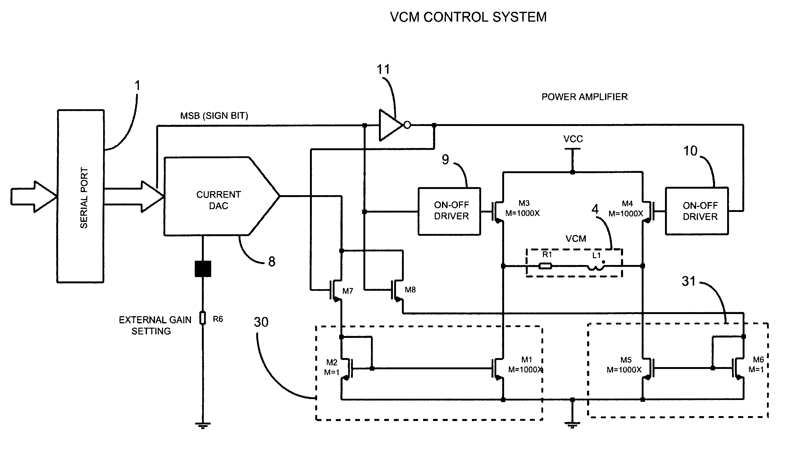
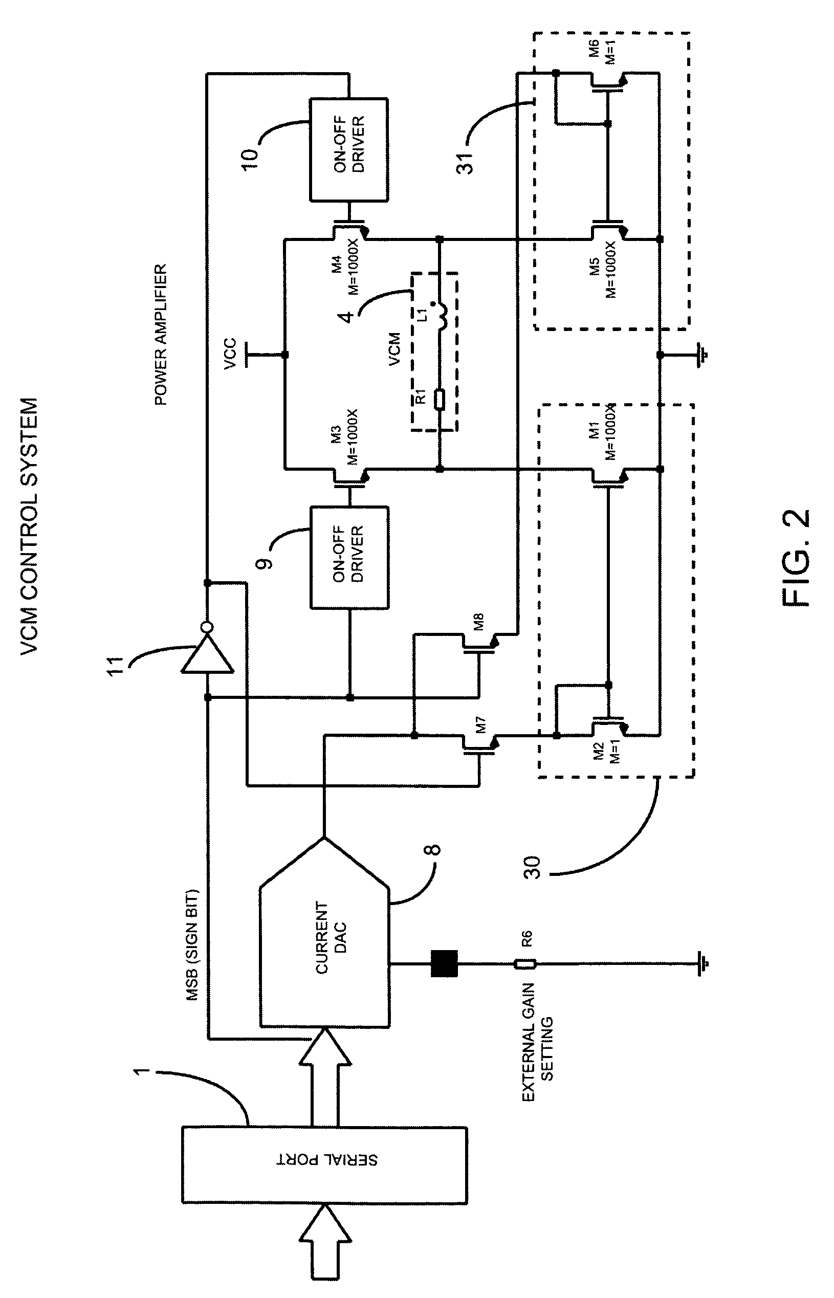
A. FIG. 2
[0068]FIG. 2 shows a general embodiment for the basic VCM driver control system utilizing a Digital to Analog Converter 8 whose output constitutes an analog current whose value is set by the digital input of the DAC 8 and by an external resistor R6. This analog current is subsequently mirrored into the full bridge to drive the desired current in the VCM actuator 4.
[0069]The full bridge is configured with two high side power transistors M3 and M4 and with two low side power transistors M1 and M5. The full bridge configuration allows the application of the full current to the load in both directions. The high side transistors may be P-type MOS devices or N-type MOS devices.
[0070]The mirroring of the current into the power devices and into the VCM load may be also implemented in several ways. In its simplest form of FIG. 2 the current mirrors 30 and 31 translate in the couples of MOS devices M2, M1 and M5, M6 sized differently in order to achieve the desired current ratio betw...
PUM
 Abstract
Description
Claims
Application Information